Ceramic Capacitor FAQ and Application Guide
Disclaimer
This document is meant to provide general answers to frequently asked questions. All information in this document is for informational purposes only and is not considered a specification.
To submit a question, please go to https://www.kemet.com/en/us/contact-us.html
General
Do MLCCs experience outgassing?
Key Words: Outgassing
KEMET Surface Mount Device (SMD) Multilayer Ceramic Capacitors (MLCCs) are constructed using high-temperature sintering processes above 1100°C-1200°C such that the final product experiences no outgassing. Although there are specifications for testing for outgassing, the current military standards for MLCCs used in space applications do not require this test. Therefore, KEMET deems it unnecessary to perform outgassing tests on MLCCs.
Note: The statement above applies to BME MLCCs with sintered copper terminations. In the case of flexible termination products, a cured silver-based soft-termination layer is applied on the copper terminations of the chips and subsequently plated with Pb-Sn or other finishes to provide additional performance benefits in board flex situations. This soft termination is adequately cured and is not expected to outgas. However, KEMET does not have testing data to support this.
How does KEMET mitigate Sn (Tin) whisker growth in MLCCs?
Key Words: Tin Whiskers
Users of MLCCs with pure tin terminations have long been concerned with possible tin whisker growth under certain application conditions. Over time, improvements in materials and processing have been implemented, dramatically reducing tin whisker growth:
- KEMET uses a matte tin finish for the plating of the termination. The matte finish does not contain any brighteners known to cause tin whisker growth.
- All MLCCs with a tin finish contain a nickel underlayer, which is a stress relief for the tin. This underlayer reduces the ability of tin whiskers to grow.
- The KEMET plating process uses a smaller grain size and slower deposition rate, which reduces the stress on the termination and thus helps mitigate tin whisker growth.
- During the plating process, each MLCC will go through a 150oC drying process for 60 minutes, which will anneal the termination. This "annealing" process will reduce the stress on the termination, thus reducing the risk of tin whisker growth.
How long can I store an MLCC?
Key Words: Storage life, oxidation
KEMET Ceramic chip capacitors should be stored in normal working environments. While the chips are quite robust in other environments, solderability will be degraded by exposure to high temperatures, high humidity, corrosive atmospheres, and long-term storage. In addition, packaging materials will be degraded by high temperature – reels may soften or warp, and tape peel force may increase.
KEMET recommends that maximum storage temperature not exceed 40°C and maximum storage humidity not exceed 70% relative humidity. Temperature fluctuations should be minimized to avoid condensation on the parts, and atmospheres should be free of chlorine and sulfur-bearing compounds. Chip stock should be used promptly for optimized solderability, preferably within 1.5 years of receipt.
Storage of MLCCs only has to do with solderability. The longer the part sits in storage, the more aggressive flux is required to solder them. After board assembly, storage conditions are recommended according to the dielectric operational temperature range to avoid any degradation in performance.
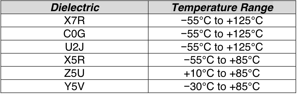
What is the Coefficient of Thermal Expansion (CTE) for MLCCs?
Key Words: Coefficient of Thermal Expansion, CTE
The coefficient of thermal expansion (CTE) refers to the rate at which a material expands with an increase in temperature. The below table shows typical values for Class I and Class II MLCCs.
Can I manually bend the leads of a leaded capacitor?
If it is necessary to bend leads for axial or radial molded components, care must be taken to prevent damage to the molding compound or lead. Follow guidelines to ensure the solderability of components and long-term reliability under operation.
- Leads should be clamped with enough force to bend the lead and not damage the plating of the lead.
- The clamp should not come into contact with the molding.
- Distance between the clamp and the molding should be greater than the lead diameter.
- Bending radius should always be greater than the lead diameter.
- Never bend leads more than 90 degrees.
- Never bend leads more than once to avoid annealing the material.
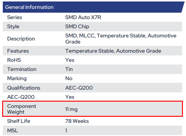
Where do I find typical piece weights for KEMET MLCCs?
Typical piece weight can be found on KEMET detailed specification sheets. See below for an example.
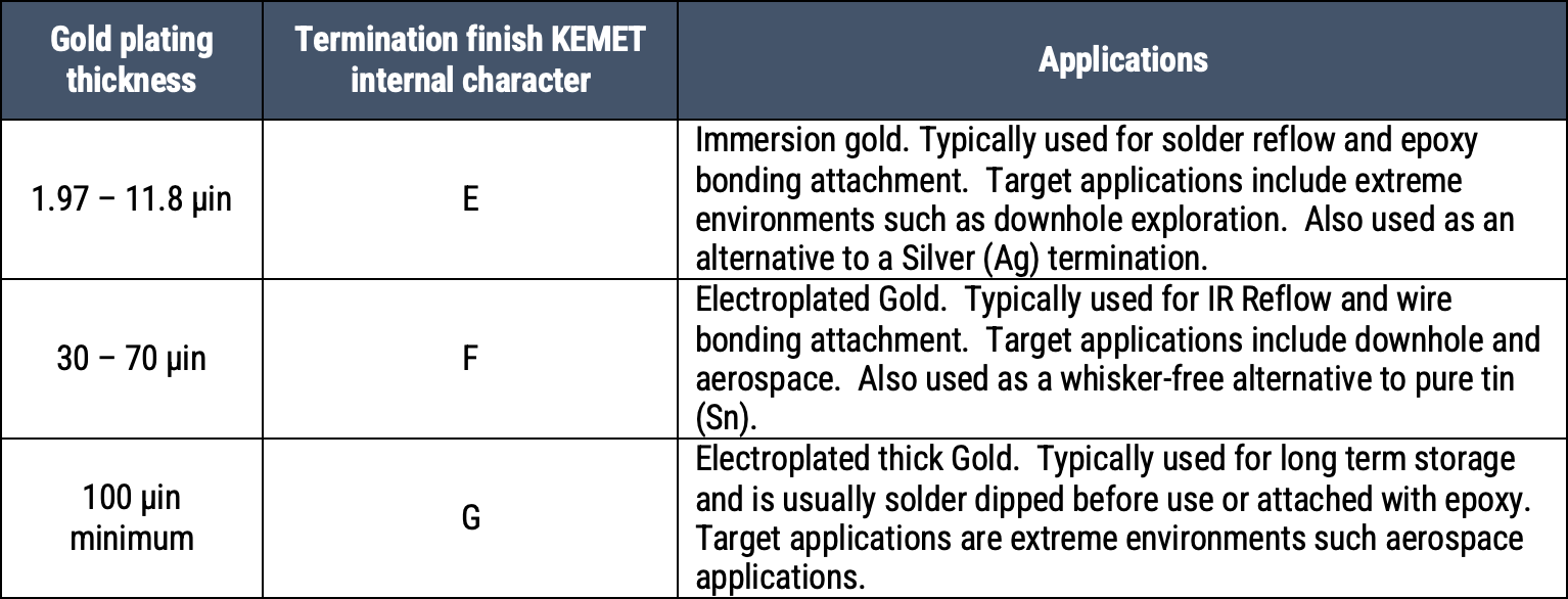
Why does KEMET offer three gold plating thicknesses?
High Temperature. KEMET Surface Mount Device (SMD) Multilayer Ceramic Capacitors (MLCCs) are specifically designed for applications in harsh environmental applications such as down hole oil exploration, industrial high temperature electronics, geothermal, and aerospace which requires capacitors that are robust and reliable at extreme temperatures. KEMET offers three different gold plating thicknesses depending on the final application. See table below.
Does KEMET offer SnPb Termination in Automotive Grade MLCCs?
The Automotive industry has moved to complete RoHS and REACH compliance for many years, which excludes the use of SnPb terminations for Automotive applications. MLCCs with SnPb terminations are not RoHS or REACH compliant. In addition, all Automotive grade MLCCs go through a custom automotive end-of-line test prior to shipment. Restricting these MLCCs to Sn terminations only prevents various processes from being contaminated with Pb and affecting Pb-free MLCCs. KEMET recommends that customers interested in SnPb terminations refer to the COTS series, which is available in both Sn and SnPb termination options.
Electrical Characteristics
What is Insulation Resistance?
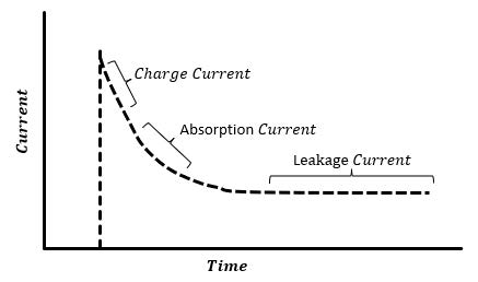
Insulation Resistance (RIns) is defined as the ratio of the applied DC voltage across an MLCC and the resulting leakage current after a specific length of time. Ideal capacitors will theoretically have a perfect insulating dielectric material and thus will have no leakage current (infinite insulation resistance) with DC voltage. However, real MLCCs will have imperfect dielectric materials, resulting in a measurable insulation resistance and leakage current.
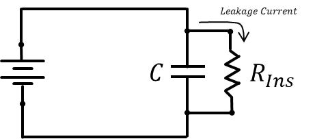
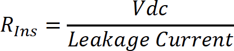
DC current through a capacitor can be separated into three regions: 1) Charging Current, 2) Absorption Current, and 3) Leakage Current. When voltage is applied to a capacitor, the initial inrush current will be due to the charging of the capacitor. Once the capacitor is fully charged, it will enter the absorption current region, which is due to ferroelectric behavior of the MLCC and the effects of polarization. Eventually, the current will reach a steady state condition where it will be constant versus time and thus is called the leakage current. The leakage current can then be used to calculate the insulation resistance of the MLCC by the equation above.
Measuring Insulation Resistance of MLCCs:
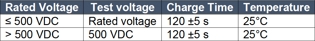
MLCCs typically have very high insulation resistances and therefore must be measured using equipment and fixtures that can accurately measure very low leakage currents. For lower capacitance MLCCs with insulation resistance in the tera-ohm range, special fixturing and cables may be required to obtain accurate readings. Insulation resistance measurements shall be made between the capacitor terminals on a megohm-meter or an insulation resistance test set. Measurements need to be made immediately after a 2-minute period of uninterrupted test voltage application and a charging current limited to 50 mA using the following measurement conditions:
Specification for Insulation Resistance
Typical insulation resistance values for MLCCs can range from Mega-ohms to 10s of tera-ohms depending on the capacitance, dielectric material, internal design, applied voltage, and temperature.
KEMET series datasheets provide specifications for the insulation resistance limit based on the case size and capacitance value. This limit is typically provided as a value in MΩ-μF units and is usually between 100 MΩ-μF and 1000 MΩ-μF depending on the series and part type.
To determine the insulation resistance limit for a specific part, divide the MΩ-μF value by the capacitance in microfarads and compare to the maximum insulation resistance limit in the datasheet (typically 10GΩ). Then select the lower of the two limits.
For example: Part Number: C1812V334KCRACTU (Commercial, X7R, 1812, 0.33 μF, 500 V)
1) From the KEMET HV X7R Commercial datasheet, select the limit according to the case size and capacitance value. For this part number, the insulation resistance limit will be 100 MW-mF or 10 GW, whichever is greater.
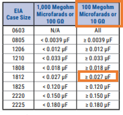
2) Divide MΩ-μF value by the capacitance value in μF.
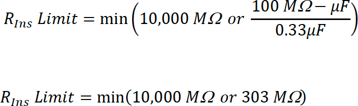
3) Select the lower of the two limits.

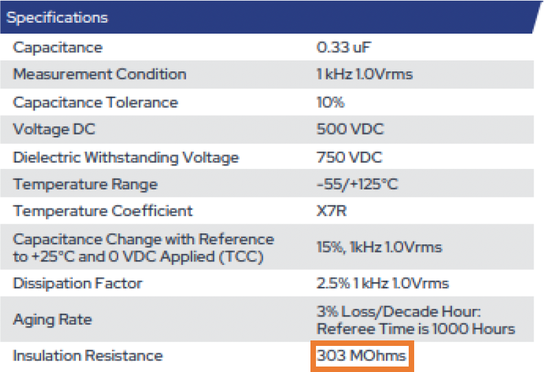
To avoid having to look up the insulation resistance limit in MΩ-μF and perform this calculation, KEMET provides the insulation resistance limit on the individual specification sheet. See below example.
What is Dielectric Withstanding Voltage (DWV)?
Dielectric Withstanding Voltage (DWV) refers to the ability of an MLCC to survive an overvoltage above its rated voltage for a short time. Another commonly used term for DWV is Voltage Proof. KEMET designs MLCCs to have a dielectric withstanding voltage capability between 1.2 to 2.5 times the rated voltage.
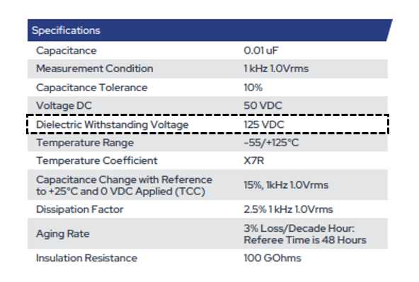
For example, KEMET X7R 0805 10nF 50V Commercial Grade MLCC has a DWV 2.5 times the rated voltage, 125V. Per the specification, the capacitor is designed to survive an overvoltage of up to 125V for no more than 5 seconds with a charging current not exceeding 50mA.
However, DWV is an indication of the overvoltage performance of an MLCC and is not meant to allow voltages higher than the rated voltage in an application. In other words, KEMET does not recommend exceeding the rated voltage per the specification sheet, even for a short time.
Since the DWV value depends on the rated voltage, see the individual specification sheet. Example below.
What is Aging for MLCCs?
Aging is a phenomenon where the capacitance of a Class II and Class III MLCC will decrease over time. MLCC aging is only related to a change in capacitance over time and is not related in any way to the lifetime or reliability of the MLCC.
What Causes Aging
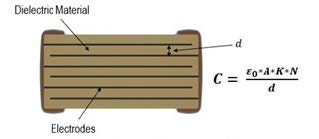
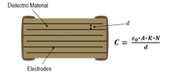
MLCCs are constructed using alternating layers of ceramic dielectric and metal electrodes. Figure 1 shows the calculation of capacitance for an MLCC where the A is the active area of the electrodes, K is the relative dielectric permittivity, N is the number of electrodes and d is the dielectric thickness. By increasing either A, K, or N, the net result will be an increase in capacitance.
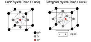
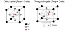
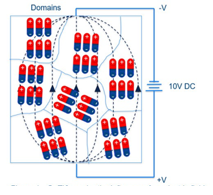
Class II MLCCs are made from a (BaTiO3) ferroelectric material which has a crystalline structure containing Barium, Titanian, and Oxygen atoms. Above its curie point (~125°C) BaTiO3 has a cubic crystal structure but as it cools down below its curie point, it transitions into a tetragonal shape. See Figure 3. The effect is an immediate spontaneous polarization of the material, forming dipoles which arrange into domain regions. The creation of the dipole is due to the shift of the titanium ion within the crystal lattice structure, causing an electric field to exist. The arrangement of the domain regions within the dielectric are randomly scattered throughout the material, in which there is no net electric polarization of the material. The electric fields of each of the dipoles cancel each other out into a neutral state. The result of the spontaneous polarization of the material is a high permittivity, which gives Class II and III MLCCs their high capacitance.
Immediately after spontaneous polarization occurs, the domains will begin to relax and realign within the material, causing a gradual decrease in the relative permittivity. The effect is a loss of capacitance over time, which is normally expressed as % Capacitance change per decade-hour after the last heat above curie point.
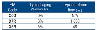
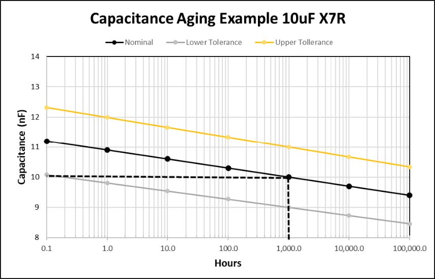
For Class II and Class III capacitors, KEMET provides Aging rate and Referee times in the part number specification sheet for all KEMET part numbers. The below table provides typical aging rates and referee times for MLCCs. Aging rates are expressed in percent and specify the amount of capacitance loss per decade-hour indefinitely. Referee time refers to the number of hours after the last heat where the capacitance is stated to be within specification. For example, for a 10uF ±5% tolerance MLCC with a referee time of 1000 hours, this means the MLCC will be within tolerance at 1000 hours after the last heat above the curie point. This is typically when the MLCCs are soldered to the PCB.
Typical Aging Rates. See Part Number Specification Sheet for actual aging rate and referee time
Special Note: Measurements before or after the referee time can show a capacitance out of specification. This is especially noticeable if measuring capacitance immediately after a soldering process. However, it is not necessary to wait until the referee time to measure the capacitance.
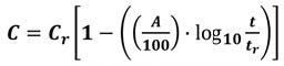
Calculating Aging Rate
By using the aging rate equation below, users can calculate the “aged” capacitance (C), based on the nominal capacitance (Cr), aging rate (A), referee time (tr), and time after last heat (t).
Can Capacitor Aging be Reset?
Yes, since Class II MLCCs are ferroelectric, once they are subjected to a temperature above the curie point, they will “deage” and the aging process will start again at 0 hours.
What is Dielectric Absorption?
In certain circuits, the capacitor's dielectric absorption is an important parameter. Dielectric absorption is the property of a dielectric, which prevents a capacitor from totally discharging, even when short-circuited for a short time. When the short circuit is removed, a small amount of DC voltage gradually reappears at the capacitor's terminals. Dielectric absorption is primarily a consideration for film capacitors in precision integrators or sample/hold circuits. It tends to increase as the dielectric constant ("K") increases. Dielectric absorption is not normally specified nor measured for ceramic capacitors. Dielectric absorption may be a more prominent consideration for low-voltage (thin dielectric) ceramic capacitors than larger voltages.
Measurement Method
- Short circuit the capacitors for 4 - 24 hours.
- Charge the capacitors to the rated voltage.
- Discharge the capacitors for 5 - 10 seconds through a 5-ohm resistor.
- Measure the maximum recovery voltage between 1 - 10 minutes, using an electrometer with an input impedance >=1010.
- Calculate dielectric absorption recovery voltage as a percentage of the charging voltage.
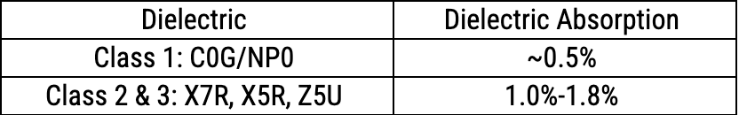
Typical Dielectric Absorption for MLCCs
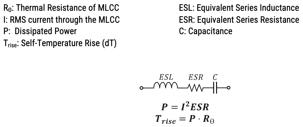
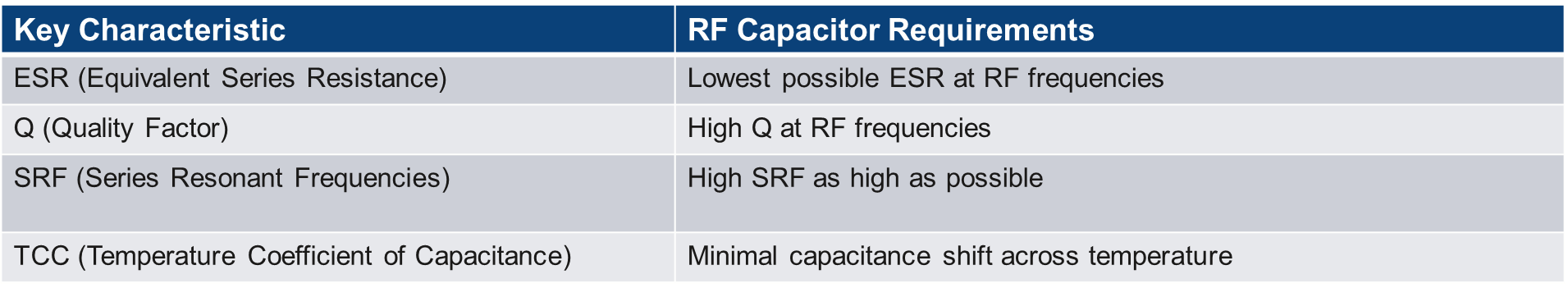
What is Equivalent Series Resistance (ESR)?
Equivalent Series Resistance, or ESR, is the sum of all the resistive losses in an MLCC and represents the fundamental part of the complex impedance equation as seen below. This equation includes the losses due to the dielectric, internal electrodes, and external terminations. For MLCCs, most resistive losses are due to the dielectric and internal electrodes. At low frequencies, the dielectric losses dominate and decrease as frequency increases. At higher frequencies, the electrode losses dominate and increase as frequency increases. MLCCs have very low ESR compared to other capacitor technologies, making them a popular choice for AC applications.
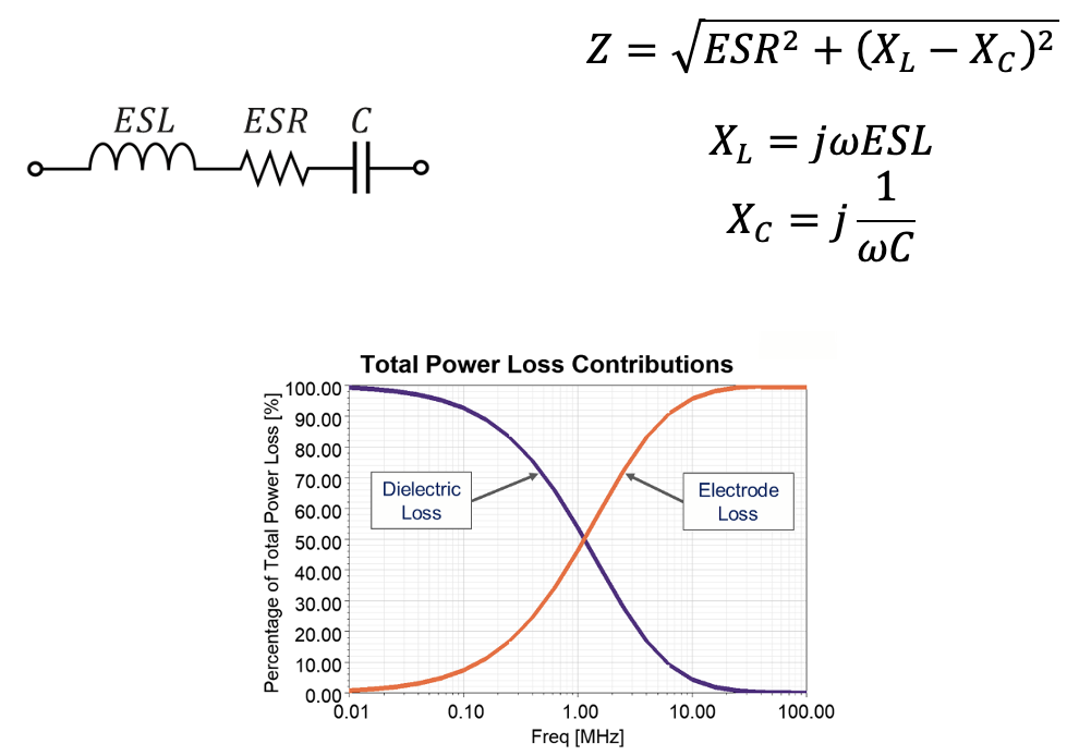
Figure 1 – Power loss contribution for dielectric and electrodes vs frequency
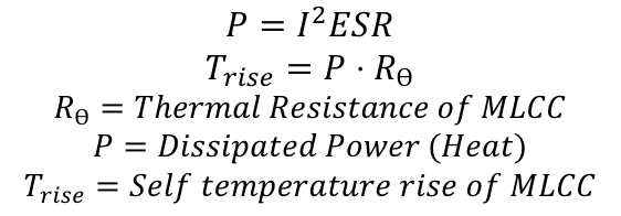
ESR is an important characteristic in MLCCs since high ESR can cause excessive power loss, resulting in thermal runaway. Since the power dissipated in an MLCC is a product of the ESR and the square of the current, higher current applications can easily cause self-heating of the MLCC.
Class 1 MLCCs such as C0G and U2J utilize a low-loss dielectric and therefore have much lower ESR than Class 2 MLCCs such as X7R, X5R, etc. Due to low ESR, Class 1 MLCCs are ideal for high AC applications such as DC-LINK, LLC resonant converters, and wireless power transfer.
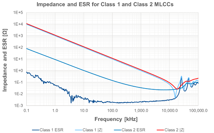
Figure 2 – Impedance and ESR vs. frequency for Class 1 and Class 2 MLCCs
The KEMET KSIM tool provides many electrical characteristics for MLCCs, including ESR.
What is Dissipation Factor (DF)?
Dissipation Factor (DF) is a measure of a capacitor’s losses under AC conditions and is defined as the ratio of ESR (resistive power loss) and reactance (reactive power). Higher DF signifies higher ESR in the capacitor causing self-heating due to I2R losses. DF is sometimes referred to as loss tangent since it represents the angle between the resistive and reactive vectors in the complex impedance graph seen below.
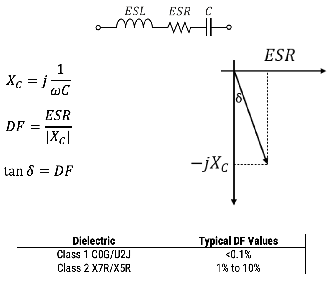
DF is measured using an LCR meter under the following conditions:
DF for KEMET capacitors can be found on the part number specification sheet.
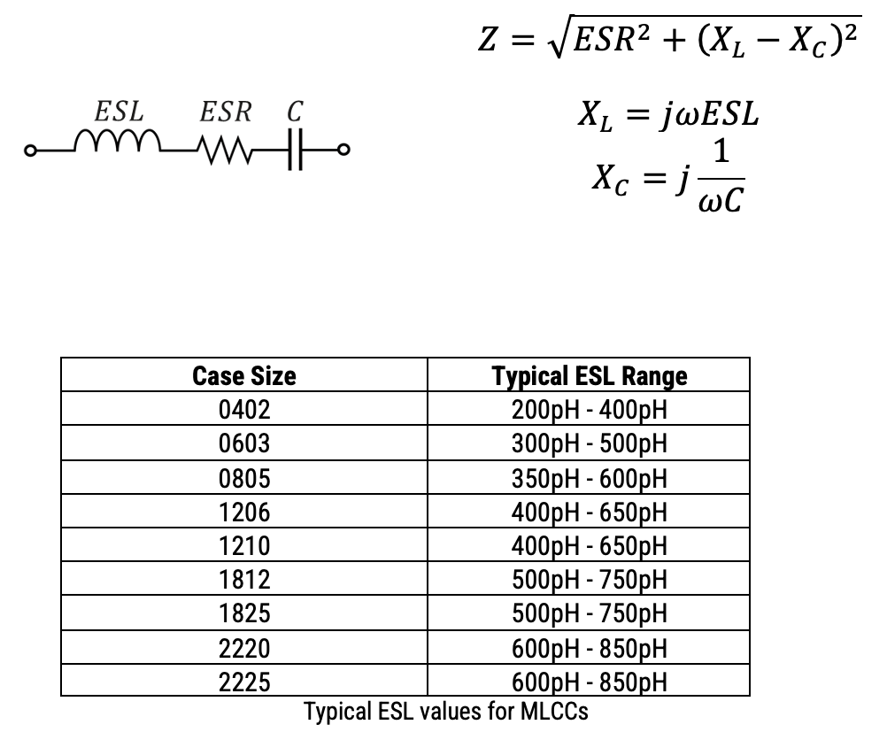
What is Equivalent Series Inductance (ESL)?
Equivalent Series Inductance, or ESL, represents the inductive reactance of a capacitor and is usually expressed in nanohenries (nH) or picohenries (pH). The simplified RLC model in the figure below shows that ESL is in series with the ESR and capacitance elements, which is why it's referred to as Equivalent Series Inductance. All capacitors, regardless of type or form factor, will have some parasitic inductance that needs to be considered, especially when used at higher frequencies. Inductance in capacitors is due to material properties and physical geometry. For example, a short and wide capacitor will have lower inductance than a long and narrow capacitor. Capacitors with leads will have much higher capacitance than surface mount (SMD).
Since MLCCs are small, surface-mount devices, their inductances are usually very low compared to other capacitor technologies. Typical ESL values for MLCCs are less than 1nH, and even as low as 0.2nH for very small EIA case sizes.
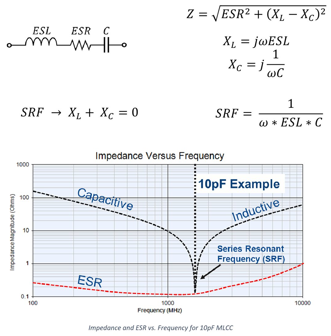
What is Series Resonant Frequency (SRF)?
Series Resonant Frequency (SRF) is the frequency where the capacitive and inductive reactances are equal in magnitude but cancel each other out leaving only ESR remaining in the impedance equation. The magnitude of the impedance for frequencies below the SRF are dominated by the capacitive reactance. Frequencies above SRF are dominated by the inductive reactance. As seen in the SRF equation below, increasing either ESL or Capacitance will result in a lower SRF.
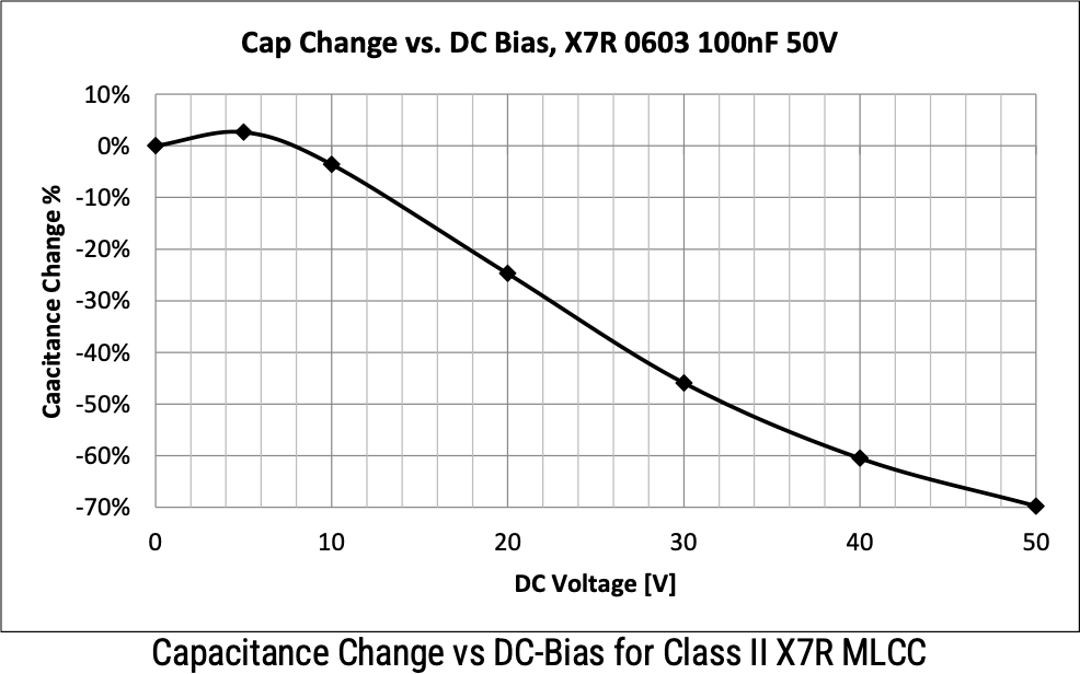
Why does capacitance change with DC voltage?
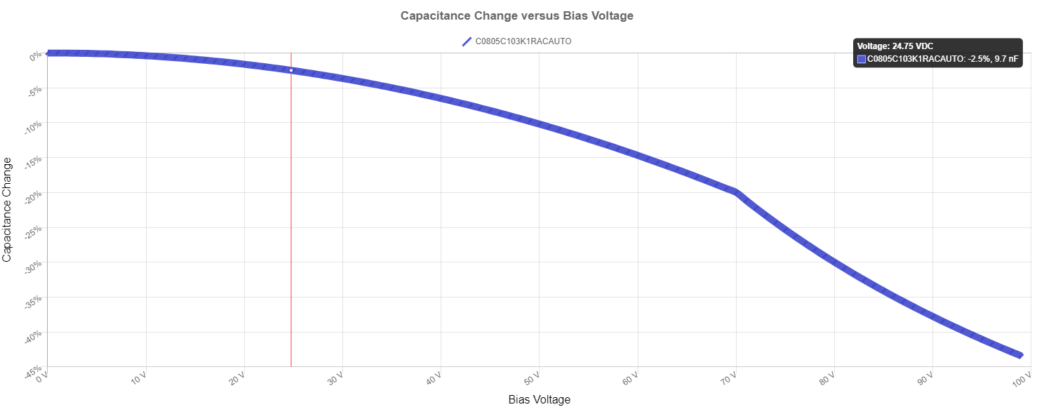
When purchasing a class II Multilayer Ceramic Capacitor (MLCC) from any manufacturer, the datasheet specifies the nominal capacitance using specific measurement parameters such as frequency, AC voltage, and DC voltage. When measuring the capacitance per the manufacturer's recommendations, the capacitance should read within the tolerance of the purchased part number. However, under applied DC voltages, there will be a noticeable decrease in capacitance in some cases up to 90% at rated voltage. (See Figure Below)
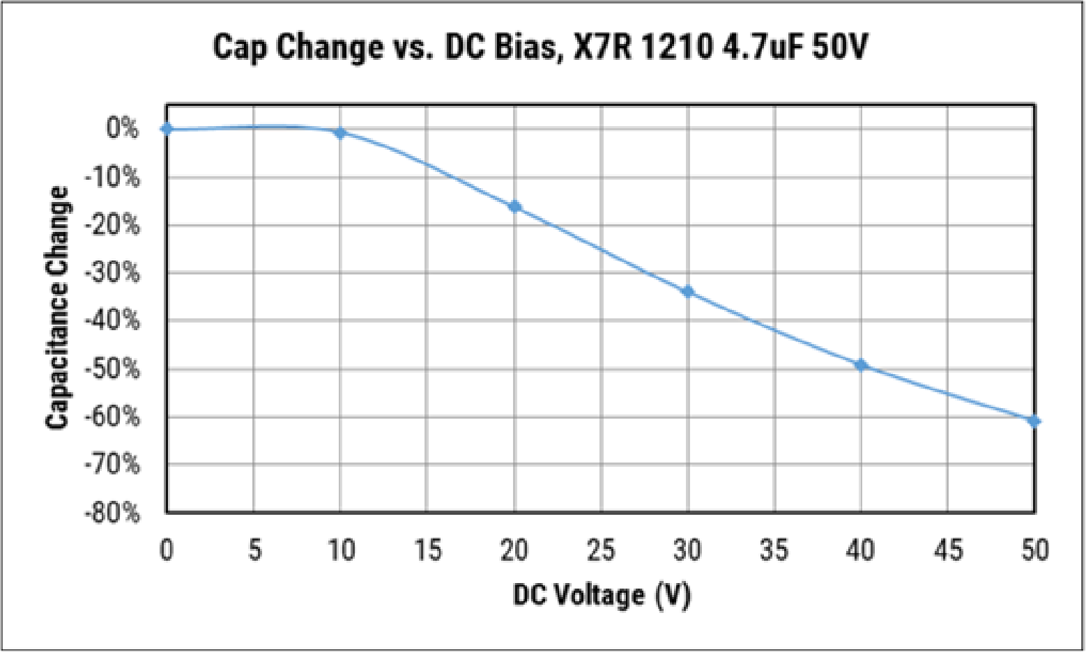
VCC is a phenomenon in Class II and Class III MLCCs, where the capacitance will decrease under applied DC voltages. This effect is most noticeable when operating at voltages close to the rated voltage and where high capacitance is a critical parameter in the design. VCC occurs in all Class II and Class III -X7R, X5R, Y5V, Z5U, etc.- capacitors from any manufacturer and is related to the design and material properties of the MLCC.
What Causes VCC?
MLCCs are constructed using alternating layers of ceramic dielectric and metal electrodes. Figure 1 shows the capacitance calculation for an MLCC where A is the active area of the electrodes, K is the relative dielectric permittivity, N is the number of electrodes, and d is the dielectric thickness. By increasing either A, K, or N, the net result will be an increase in capacitance.
Class II MLCCs are made from a (BaTiO3) ferroelectric material, which has a crystalline structure containing Barium, Titanian, and Oxygen atoms. Above its curie point (~130°C) BaTiO3 has a cubic crystal structure, but as it cools down below its curie point, it transitions into a tetragonal shape. See Figure 3. The effect is an immediate spontaneous polarization of the material, forming dipoles which arrange into domain regions. The creation of the dipole is due to the shift of the titanium ion within the crystal lattice structure, causing an electric field to exist. The arrangement of the domain regions within the dielectric is randomly scattered throughout the material, in which there is no net electric polarization of the material. The electric fields of each dipole cancel each other out into a neutral state. The result of the spontaneous polarization of the material is a high permittivity, which gives Class II and III MLCCs their high capacitance. During a capacitance measurement using small AC voltages, the titanium ion is free to move with the alternating electric field.
When DC voltage is applied to the MLCC, an electric field would be present throughout the dielectric, and the titanium ion would now be influenced by both the DC electric field and AC electric field. As the DC voltage increases, the titanium ion becomes "locked" into place, preventing it from being influenced by the AC voltage, thus reducing the material's dielectric constant. This results in a measurable drop in capacitance in the MLCCs.
Factors Influencing VCC
Not all Class II and Class III MLCCs will have the same level of capacitance loss versus DC voltage. Some MLCCs may lose 10% capacitance at rated voltage, while another MLCC of the same case size may lose 70% at rated voltage. Two factors influence VCC:
- Applied Voltage – As voltage increases on an MLCC, higher electric fields are present on each active layer. Therefore, as voltage increases, capacitance loss also increases.
- Dielectric Material – Class II and III MLCCs are made from BaTiO3 material but include other materials, such as dopants, to improve performance, quality, and processing. Formulation differences between MLCCs can have a significant impact on VCC.
- Design – MLCCs are constructed using alternating ceramic dielectric and metal electrode layers (Figure X). The dielectric thickness (separation between the electrodes) can range from 10μm down to below 1μm. As the dielectric thickness decreases, the electric field on each MLCC layer increases, thus increasing the effect of VCC.
What about Class I MLCCs?
Class I MLCCs are made from CaZrO3 dielectric, a paraelectric material. Therefore, Class I MLCCs are stable and have almost no capacitance shift with DC or AC voltage.
Where to find VCC for your MLCC?
The KEMET KSIM tool provides designers with electrical characteristics such as Impedance, ESR, VCC, VCAC, TCC, S-Parameters, and Ripple Current. Go to https://ksim3.kemet.com/
In addition to the KEMET KSIM tool, detailed specification sheets also provide electrical characteristics.
Why does capacitance appear to be out of tolerance when I measure it?
Overview
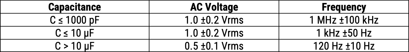
Many instruments can be used to measure the electrical properties of capacitors. When measuring capacitance, these instruments apply a known AC voltage and frequency across the capacitor (device-under-test [DUT]) to measure the corresponding impedance. The capacitance is then extracted from the impedance measurement. The table below illustrates the voltage and frequency parameters recommended for measuring Class-II and Class-III ceramic capacitors.

Table 1 – Measurement of voltage and frequency by the capacitance value
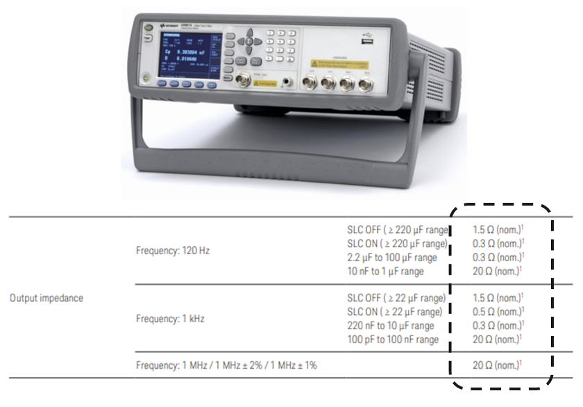
Output Impedance of the Instrument
All capacitance measurement equipment will have a known output impedance greater than zero. The output impedance will vary based upon the model and/or capacitance measurement range of the equipment. Impedance is a critical factor in the measurement of capacitance, especially when the impedance of the device under test (DUT) approaches the impedance of the instrument. The figure shows the general schematic of a capacitance measurement with the instrument source impedance.
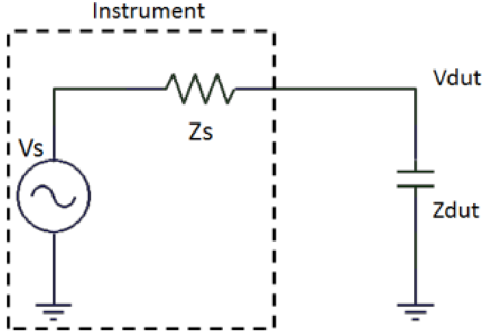
When a DUT is being measured for capacitance, the source voltage of the test equipment must be set to the desired measurement voltage. In the case of a 10uF capacitor, the source voltage would be 1.0 Vrms based on the table above. If the instrument's output impedance is high enough, it will cause a voltage divider and reduce the actual test voltage across the DUT. The equation below shows the voltage across the DUT during the measurement. From the equation, we can see that as the source impedance (Zs) approaches the impedance of the DUT, there will be a voltage drop across the part. Using this equation, we can plot the percent voltage drop across the DUT during measurement as a function of capacitance, as shown in the voltage versus capacitance graph. The graph below illustrates a drop in voltage at around 100nF, with only 15% of the voltage at 10uF. The voltage steps up to around 80% just after 10uF due to the change in frequency.
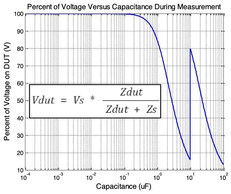
From Table 1, the desired voltage and frequency are 1.0 Vrms and 1 kHz, respectively. In this example, the output impedance of the test meter is 100 Ohms based on the meter's specifications. At 1 kHz, the DUT impedance will be 15.91 Ohms. Using the voltage divider equation, the voltage across the DUT will be approximately 157 mV. Thus, only about 15% of the output voltage is actually applied to the DUT. Because of the resulting voltage drop across the DUT, the capacitance measurement is invalid since it does not meet the test specifications outlined in Table 1. It is important to maintain a constant test voltage while measuring capacitance. Figure 3 shows an actual measurement of a 10uF capacitor using the Agilent E4980 LCR meter. The measured AC voltage across the capacitor is only 186 mV, far below the 1 Vrms specification. The test result falsely indicates that the capacitor does not meet its rated specification. The following section will show how to correct for this anomaly and limitation.
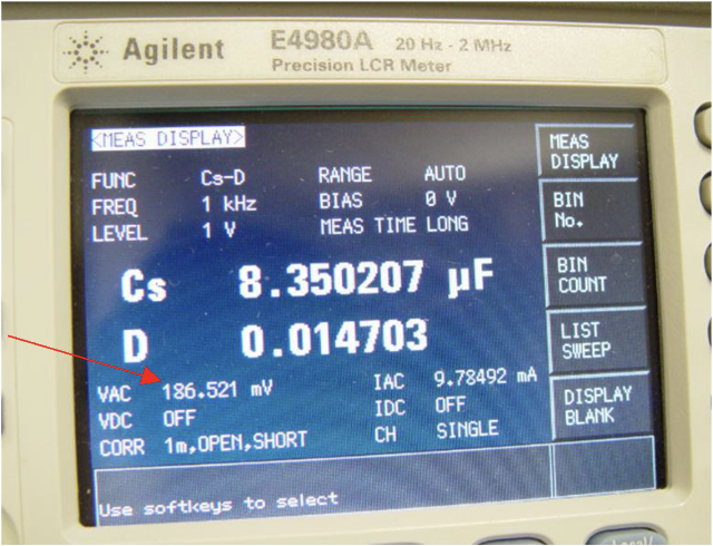
Capacitance measurement of 10uF capacitor with ALC off
How do we correct for the voltage drop?
To ensure the voltage across the DUT is maintained at the desired level, the output voltage needs to be increased on the test meter to adjust for the voltage divider. Some capacitance measurement equipment will have a function called Auto-Level Control (ALC) which does this automatically. This feature enables the instrument to automatically increase the source voltage to meet the set voltage. When considering the case in Example 1 above, without the ALC function, the voltage across the DUT was 186 mV with a set voltage of 1.0 Vrms. If we enable the ALC function, the instrument will automatically raise the source voltage to achieve the desired 1.0 Vrms across the DUT. Figure 4 shows a measurement of the same 10uF capacitor using the Agilent E4980 LCR meter with the ALC feature set to ON. The test result shows the capacitor measures within the 10% tolerance range.
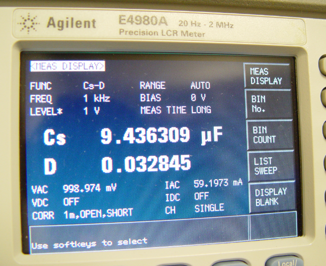
Capacitance measurement of 10uF capacitor using ALC function
Is the ALC function the only way to avoid this issue?
No, other methods exist to avoid a voltage drop during the capacitance measurements. Per the voltage divider equation above, as the source impedance decreases, so does the voltage drop. To solve this, impedance measurement equipment suppliers such as Keysight Technologies provide LCR meters with much lower source impedances, such as the E4981A Capacitance Meter. Due to the very low source impedance, the ALC function is not necessary.
Aspects of Class-II and Class-III Dielectrics
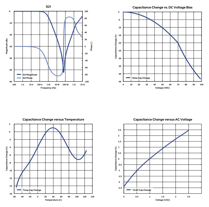
The measured capacitance of Class-II (X7R, X5R, X8R, etc.) and Class-III (Y5V, Z5U, etc.) devices will change if the applied voltage increases and decreases. The relative permittivity of these dielectric materials is affected by both AC and DC voltage. The severity of the change depends on the magnitude of the voltage, the dielectric type, and the thickness of the dielectric. Figure 5 illustrates typical capacitance change versus AC voltage of a Class-II capacitor. Figure 6 illustrates typical capacitance change versus DC voltage on a 16VDC-rated part. Based on the plots in Figures 5 and 6, it is important to note that AC and DC applied voltages must be considered when measuring capacitance.
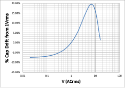
Capacitance versus AC Voltage
Mounting and Handling
Is it OK to hand-solder MLCCs using a soldering iron?
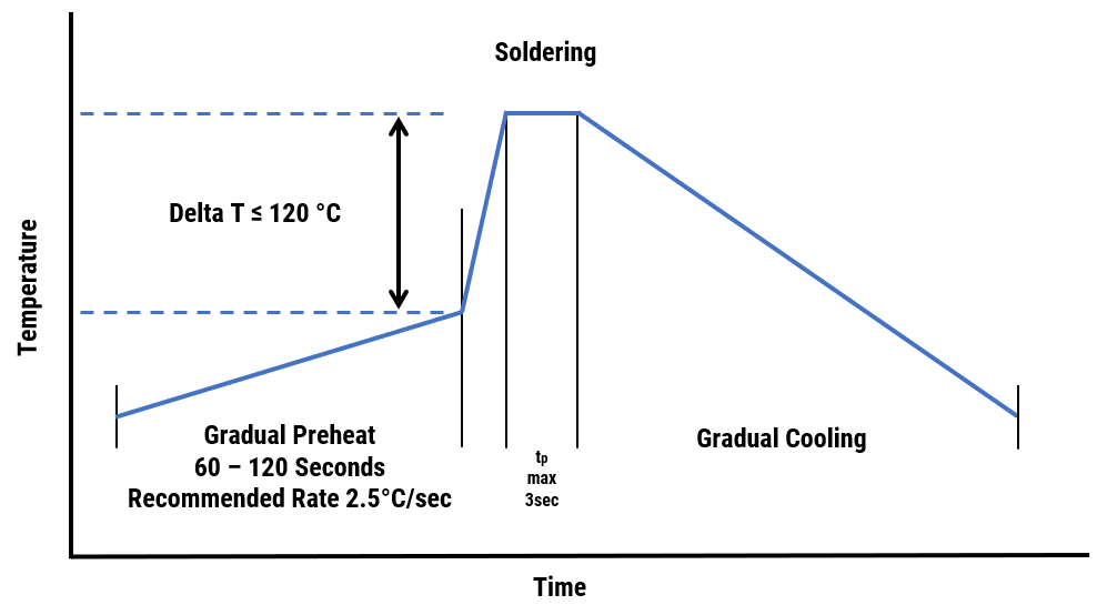
Since MLCCs utilize ceramic dielectric material, they are prone to cracks due to excessive temperature gradients. Therefore, care must be taken when employing hand soldering techniques to prevent temperature gradients. Below are some guidelines to help mitigate the risk of thermal cracks during the hand-soldering process. This process is not recommended for case sizes larger than EIA 1210.
Guideline 1: With Pre-Heating
- Utilize 1.0mm thread eutectic solder with soldering flux in the core. Either a rosin-based or nonactivated flux is recommended.
- The capacitors shall be pre-heated so that the temperature gradient between the devices and the tip of the soldering iron is Delta T<=120°C or below.
- The temperature of the solder iron tip should not exceed 300°C.
- The required amount of solder shall be melted in advance on the soldering tip.
- After soldering, the capacitors shall be cooled gradually at room ambient temperature. Forced air cooling is not permitted.
Guideline 2: Without Pre-Heating
- The soldering iron tip shall never directly touch the capacitors' ceramic dielectrics and terminal electrodes.
- Lands are sufficiently pre-heated with a soldering iron tip before sliding the soldering iron tip to the terminal electrode of the capacitor for soldering.
What is the recommended cleaning procedure for MLCCs after mounting?
To clean MLCCs after the assembly process:
KEMET recommends solvents like isopropyl alcohol (IPA), ethanol, deionized water, and other standard PCB cleaning solutions such as Oakite, Okemclean, Biokleen, PINE ALPHA cleaners (Arakawa), Clean through series cleaners (Kao), etc. Aggressive solvents are not recommended.
MLCCs should be cleaned thoroughly with no remnants of flux residue.
Insufficient washing might leave traces of flux residue causing degradation of the electrical properties of the capacitor, such as its insulation resistance.
If using Ultrasonic cleaning, KEMET recommends the guidelines below:
Ultrasonic Power: 20 W/ℓ maximum
Ultrasonic Frequency: 20 kHz - 40 kHz
Ultrasonic Temperature: 60°C / 140°F maximum
Ultrasonic Cleaning Duration: 5 minutes maximum
While using Ultrasonic cleaning, it is important to consider that excessive vibration of PCBs or resonance between mounted components and the PCB may cause cracking in the solder joints or capacitors. KEMET recommends testing your cleaning process on the final production PCB to validate its suitability for the capacitors and PCBs used.
Do Ceramic Capacitors have an MSL Rating?
The Moisture Sensitivity Level (MSL) indicates how long an electrical component can be exposed to ambient humidity before it becomes compromised during the reflow soldering process. Some components are very sensitive to humidity and require moisture-sensitive packaging for short- and long-term storage. During the reflow process, the entrapped moisture will become gas, violently expanding and damaging the component. Since not all electronic components will absorb moisture at the same rate, the MSL defines the risk for the component and the time the component can be at ambient room conditions prior to reflow. If the time at ambient conditions is exceeded, the components must go through a baking (drying) cycle. Most manufacturers classify components to an IPC/JEDEC Joint Industry Standard (J-STD-033) per the table below.
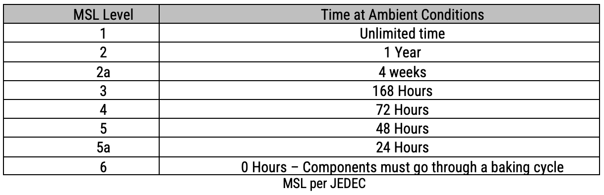
All MLCCs are not sensitive to ambient humidity and have an MSL rating of 1. Baking is unnecessary.
Note: MSL rating is not related to storage life. The storage life of MLCCs is due to oxidation of the terminations only, which affects solderability and is typically within 1.5 years of receipt. Please see the KEMET datasheet for actual storage life specifications.
How long can MLCCs be stored once soldered to a PCB?
KEMET provides guidelines for storing MLCCs on each datasheet. Depending on the product, storage guidelines for MLCCs are typically 6-18 months. However, the storage requirement is only for MLCCs prior to soldering to a PCB. The storage requirements for MLCCs are due to oxidation of the external tin (Sn) termination finish that may reduce solderability. Staying within the KEMET guidelines for storage will ensure optimum solderability. However, once the MLCC is soldered to the PCB, there is no concern with oxidation, and therefore the mounted MLCCs can be stored indefinitely.
Flex Mitigation
How do I reduce the chances of failures due to flex cracks?
Reduce Board Flex
Ceramic materials are inherently brittle and may crack under excessive strain. Therefore, it's important not to apply excessive bending on the PCB during the manufacturing process, which can induce flex cracks. One key area of the manufacturing process that can induce excessive board flex is PCB depanelization/singulation. KEMET recommends applying a strain gauge analysis during process development.
Beware of high-risk areas of the PCB.
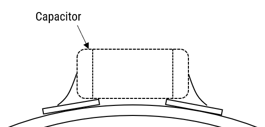
Connectors – MLCCs placed close to connectors are at risk of flex cracks. When connectors are attached to the PCB, excessive force may be applied, inducing flex stress on the MLCCs.
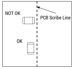
Close to the edge of PCB or near scribe lines for depanelization – During depanelization, MLCCs close to the edge may see more flex compared to areas further away. Consider mounting MLCCs parallel to the edge of the PCB to reduce the risk of flex cracks.
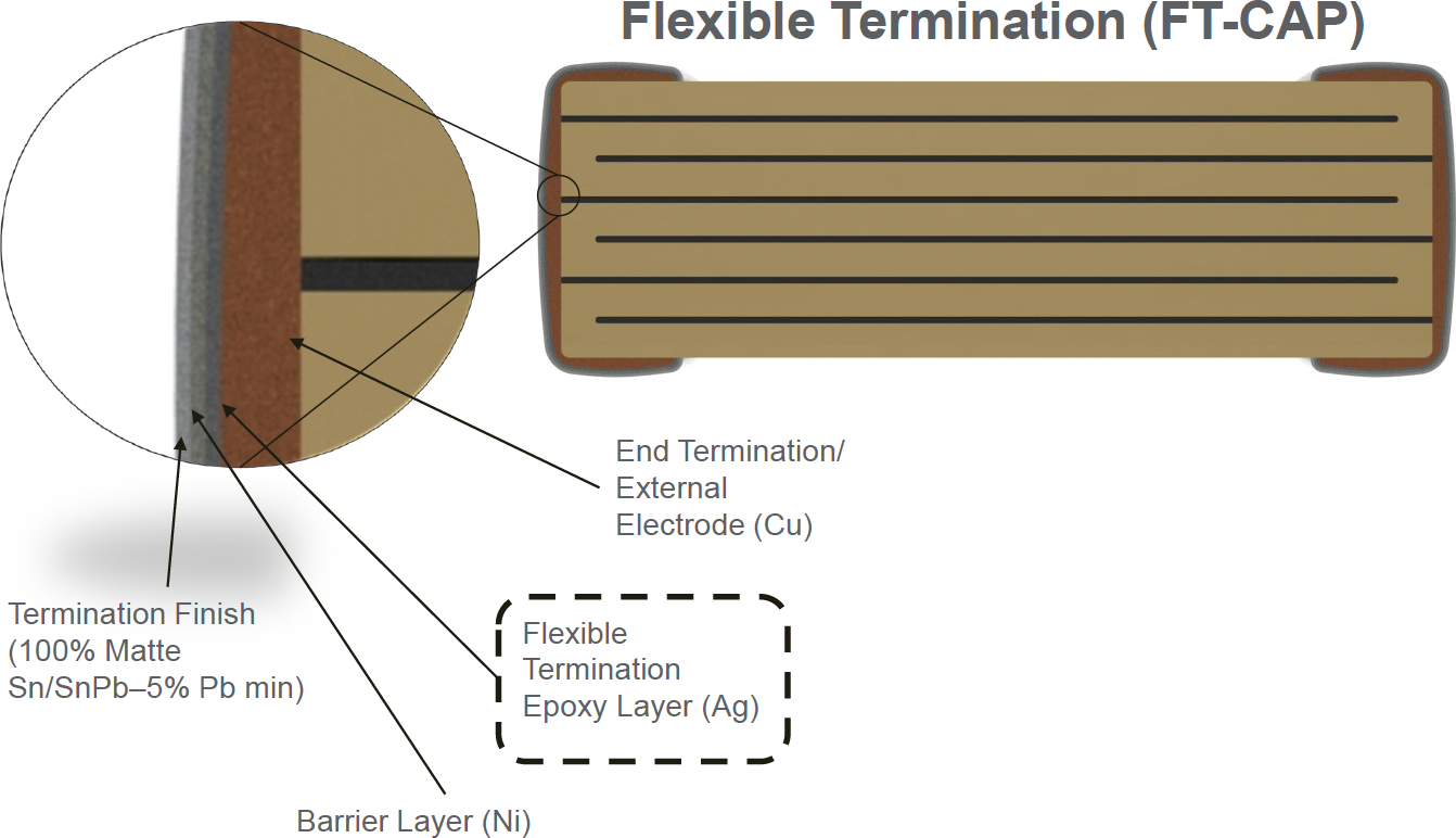
How does Flexible Termination reduce the risk of flex cracks?
When MLCCs are mounted to PCBs, excessive board strain can lead to excessive stress on the MLCC, leading to flex cracks and short circuits. Therefore, to alleviate this stress, KEMET offers a flexible termination option that can drastically improve flex robustness.
KEMET Flexible Termination is a layer of highly conductive silver epoxy between the copper termination and the nickel barrier layer. This silver epoxy layer helps mitigate the risk of flex cracks by the following two methods:
• The silver epoxy layer acts as a soft and compliant material between the copper and nickel layer that will absorb the mechanical board strain, limiting the stress on the MLCC.
• Under extreme board strain, the silver epoxy may tear from the copper termination, acting as a mechanical fuse. Although this may result in decreased performance from the MLCC, it will reduce the likelihood of a short circuit.
KEMET flexible termination MLCCs provide up to 5mm capability from EIA 0402 – 1210 case sizes and 3mm capability for larger case sizes.
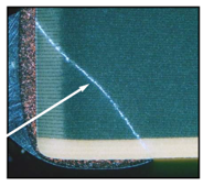
Does a flex crack always have the same crack signature?
Yes, a distinctive crack signature for board flex cracks always starts near the edge of the termination margin and usually extends upwards toward the termination face. The flex crack signature distinctly differs from other crack signatures in MLCCs.
Typical Flex Crack
Do flex cracks always result in immediate short circuits?
No, as with all cracks in MLCCs, there needs to be some ionic penetration or humidity along the crack path, which allows current to flow between electrode plates of opposite polarity for the chip to fail.
Does KEMET ever ship capacitors with flex cracks while still in the tape and reel?
No. Since MLCCs require excessive strain to induce a flex crack, this can only occur after the mounting process.
High Voltage
How do I reduce the risk of arcing in high-voltage applications?
Coating for High Voltage MLCCs
For MLCC ratings ≥1500V, it is recommended to apply a conformal coating to MLCC to prevent surface arcing. To reduce the possibility of inducing cracks in the MLCC, select a coating with thermal expansions close to that of the MLCC.
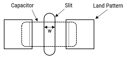
Slits in PCB
It is recommended to apply a slit in the PCB under the MLCC to improve the washing of flux residue.
- Recommended for case sizes ≥1206
- The width (w) of the slit should be 1mm
- The length of the slit should be as short as possible to prevent damaging the MLCC due to the mechanical stress of the PCB.
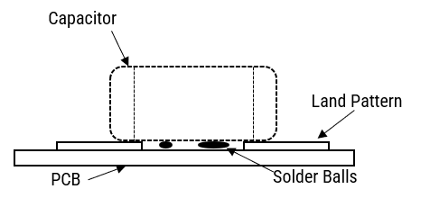
- Slits also reduce the risk of solder balls under MLCC, which decreases the creepage distance.
Solder Balls
Improper reflow techniques and/or improper washing can induce solder balls under or adjacent to the MLCC. Solder balls reduce the creepage distance between the MLCC terminations and increase the risk of arcing or damage to the ceramic material. To reduce the risk of solder balls:
Follow KEMET solder recommendations as outlined in the datasheet.
If performing a cleaning procedure, properly clean the PCB per KEMET cleaning recommendations.
Add a slit to the PCB, as shown above.
Electrostatic Discharge (ESD) Rated MLCCs
What is ESD?
ESD, or Electrostatic Discharge, refers to the release of static electricity when two objects come into contact. Electrostatic discharge voltages can be as high as 30kV and produce currents of 30 amps in some cases. However, the total energy of ESD transient pulses is very low (<50mJ) and occurs in less than 100ns. Therefore, ESD is usually harmless to people, but can have very negative effects on electronics. If protective measures are not utilized in PCB handling and design, ESD pulses can damage sensitive electronic components, impacting overall system reliability.
How Does KEMET Test MLCCs for ESD Susceptibility?
KEMET tests MLCCs per AEC-Q200, Human Body Model as shown in the discharge network below. During this test, the high voltage power supply charges Cd through a charge resistor Rch. Once capacitor Cd is fully charged, the high voltage relay is closed discharging Cd into the Capacitor Under Test through the discharge resistor Rd. For ESD testing per AEC-Q200, Cd=150pF and Rd=2000 Ohms.
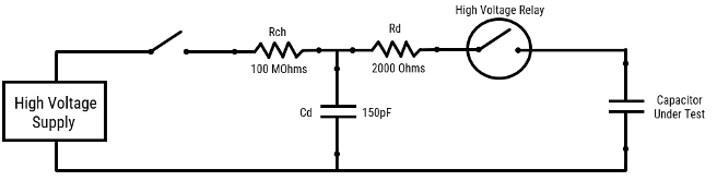
Discharge Network for ESD Testing per AEC-Q200
The typical ESD waveform produced using this network is shown below.
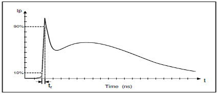
Typical ESD Waveform
Per AEC-Q200, each part type is tested using the below classification tree in order to establish the MLCC’s final ESD class.
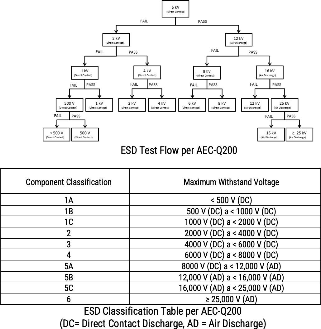
For ESD classification per IEC 61000-4-2, please contact KEMET.
Does KEMET offer MLCCs with an ESD Rating?
MLCCs are typically not designed to maximize ESD performance and do not receive in-process testing to maintain a specific ESD rating. Therefore, KEMET standard Commercial and Automotive Grade products do not have a published ESD rating.
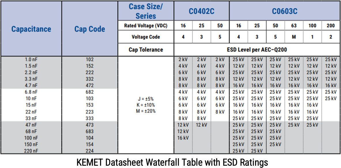
However, KEMET does offer an ESD rated series in both C0G and X7R dielectrics for Commercial and Automotive applications. There are four characteristics that make KEMET ESD series specifically for ESD applications:
- Designs are optimized to maximize ESD rating.
- Designs are controlled to maintain the ESD rating throughout the product lifecycle.
- Samples from each batch are tested for ESD before shipment.
- ESD rating is provided on the family datasheet and individual specification sheet, as seen below.
Why are MLCCs used for ESD Suppression?
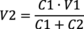
MLCCs are a common choice for ESD suppression due to their small case size, low cost, and effectiveness in protecting sensitive integrated circuits. MLCCs suppress ESD by absorbing the charge from the source of the ESD. To illustrate this concept, below are two images showing a capacitor C1 being discharged into capacitor C2 through a switch. In the picture on the left, capacitor C1 is charged to V1 and establishes a charge Q1. Since ESD sources (such as the human body) have a relatively low capacitance, the resulting charge Q1 will also be low. When the switch is closed, C1 is discharged into C2 (which represents an MLCC used to suppress ESD transients). After the switch is closed, the corresponding charge from C1 now must be shared between C1 and C2. From the equation on the right, as C2 increases, the resulting voltage across C2 will also decrease. Therefore, higher capacitance values of C2 will offer much better ESD protection compared to lower capacitance values.
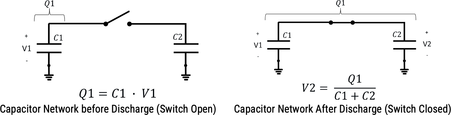
By substituting C1 * V1 for Q1 in the equation on the right, we can now calculate the resulting ESD voltage based on the capacitors and ESD charge voltage.
Below is a graph of the resulting ESD voltage versus ESD MLCC capacitance when applying a 25kV ESD source voltage and 150pF source capacitance. The results show a significant decrease in resulting voltage versus capacitance.
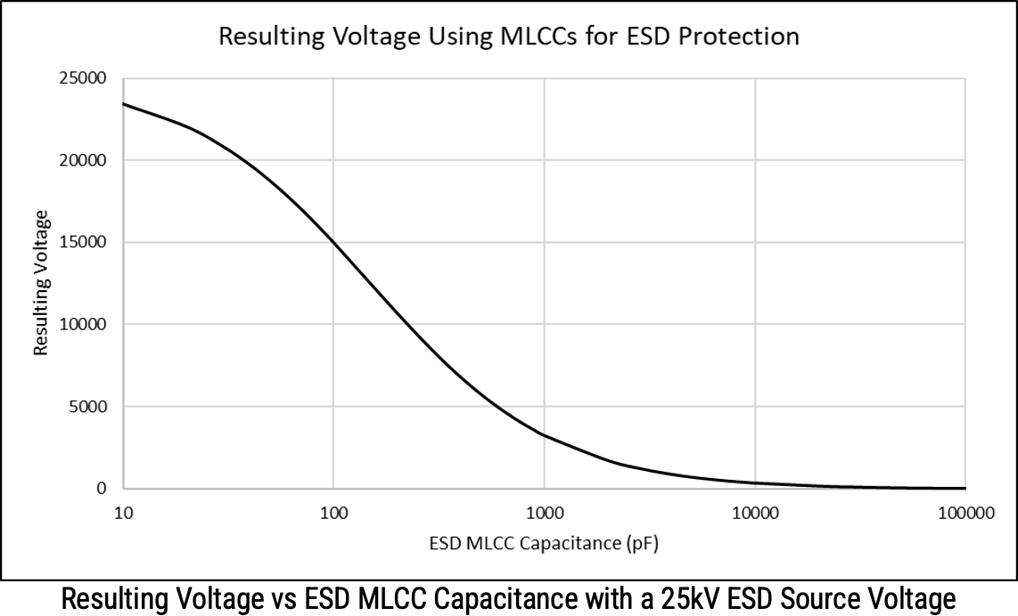
A key consideration in selecting MLCCs for ESD suppression is taking into account the capacitance change versus DC-Bias. For details on this phenomenon, see question Why Does Capacitance Change with DC Voltage? As voltage increases on the MLCC, the capacitance will decrease, reducing the effectiveness to absorb the ESD charge. Therefore, it is recommended to use the KEMET KSIM tool to evaluate the worst-case capacitance and impact on the resulting voltage from the above equation.
DC and AC Voltage Considerations
What is the maximum AC voltage I can use on a DC-rated MLCC?
KEMET Surface Mount Device (SMD) Multilayer Ceramic Capacitors (MLCCs) are normally rated at DC voltages. However, in many cases, applications require AC voltages that can be high enough to cause degradation. The below guidelines can be used to convert the DC-rated voltage to max allowable AC voltage.
Guidelines for AC Voltage
Definitions:

When calculating the AC-rated voltage of an MLCC, both Guideline #1 and Guideline #2 below must be followed.
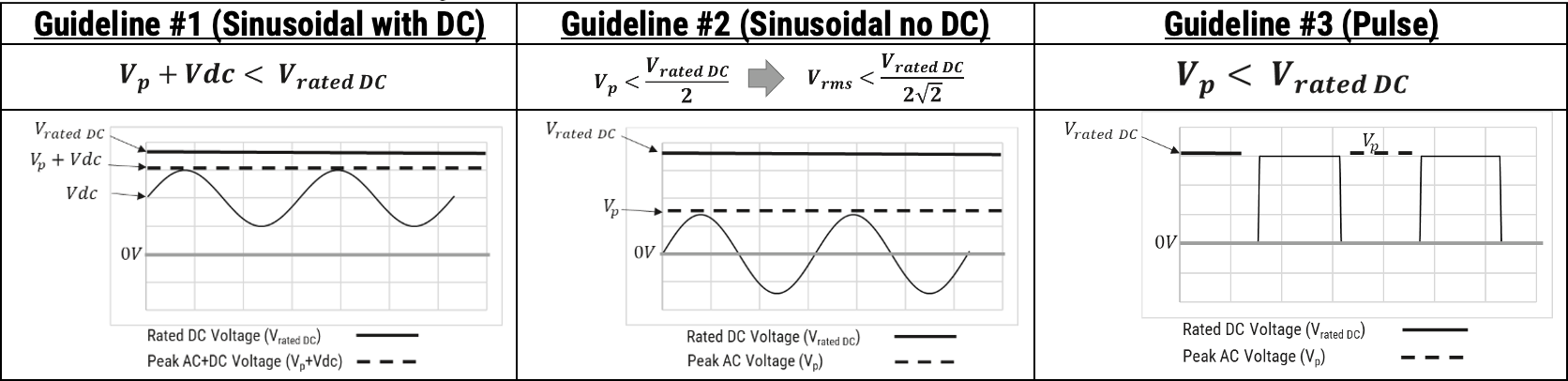
When AC voltage is superimposed on DC voltage, the total voltage (Vp+Vdc) must be less than the DC-rated voltage of the MLCC.
If a transient or pulsed voltage is applied, it must be below the DC-rated voltage of the MLCC.
Guidelines for AC Current
In addition to the guidelines above, KEMET recommends that the max temperature of the MLCC never exceed the operating temperature during the lifetime of the application.
Definitions:
Note that these are only guidelines and do not serve as an absolute AC voltage and current rating of the MLCC in the application. Validation of the MLCC under full power operation is still required to assess product capability.
Is it safe to use ceramic capacitors above their rated voltage?
Key Words: Derating
MLCCs are designed and tested to be used up to full rated temperature and voltage per the datasheet and specification sheet. KEMET does not recommend exceeding the rated voltage or temperature, even briefly.
Do KEMET ceramic capacitors require voltage derating?
It is common for some capacitor technologies, such as Tantalum and Film, to require voltage derating at elevated temperatures. Even when used within the capacitor's maximum operating temperature, these capacitors may require a reduced voltage to maintain reliability.
However, KEMET ceramic capacitors are designed and qualified to operate at full-rated temperature and voltage. For example, an X7R 100nF 50V rated MLCC with an operating temperature of 125°C can be used at 50V and 125°C. No derating is required.
Safety Certified Ceramic Capacitors
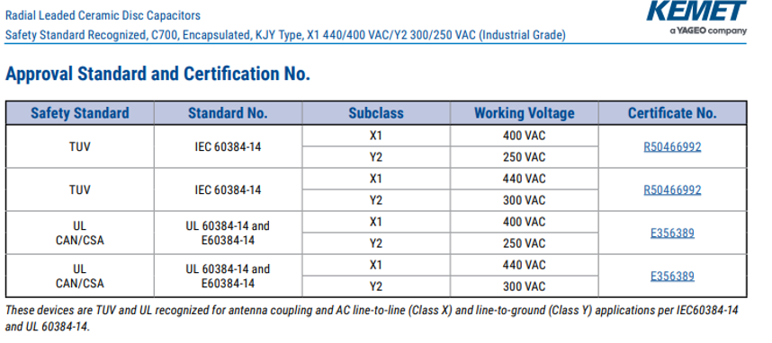
Where can I find safety certificates for KEMET products? Can I obtain a CB report?
Safety certifications for KEMET Safety Certified products can be found in two locations:
KEMET.com > Support > Quality Documents and Certificates
Please see Product-Level Certificates pertaining to the series of interest.
Here you are able to view and download a PDF of our safety certification which demonstrates our compliance to IEC 60384-14.
Or in the individual product family datasheets:
Can a Y2 capacitor be used in place of a Y1?
No, you cannot use a Y2 in place of a Y1. However, you can use a Y1 in place of a Y2. Both X2 and Y2 are primarily used in residential applications and do not necessarily require the mitigation of much higher impulse voltages that industrial applications tend to see. The table below shows the sub-classification per IEC 60384-14, which specifies the peak impulse that each subclass can handle. Intuitively, the Y2, which is tested at 5kV peak impulse, is not rated to comply with Y1's rating of 8kV.
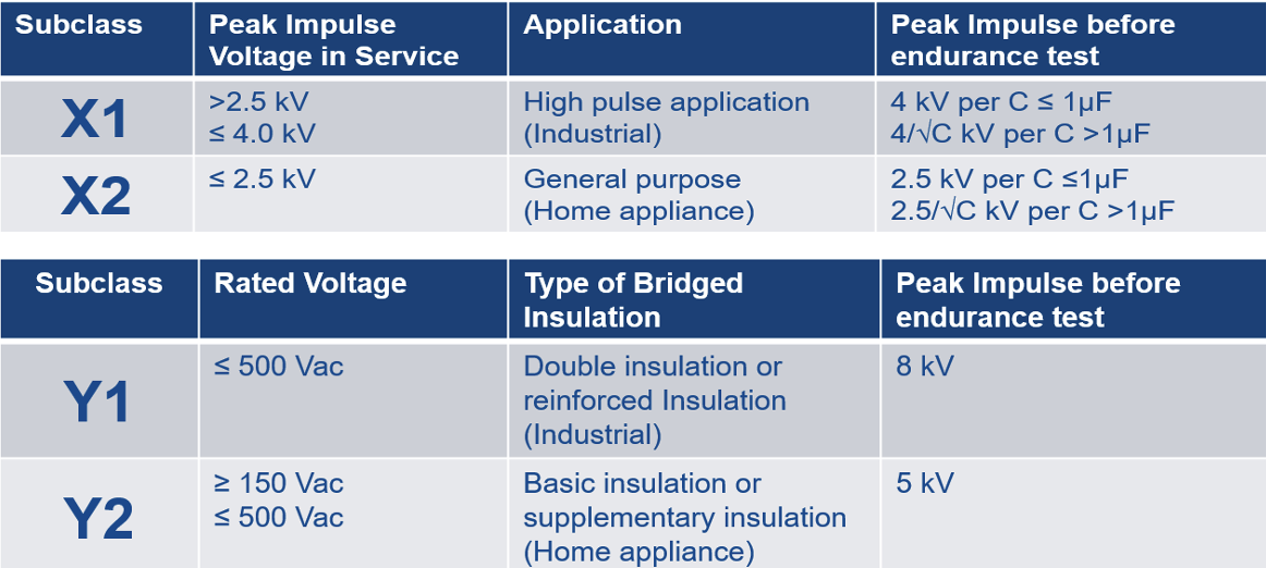
Please consider this matrix when determining substitutions.
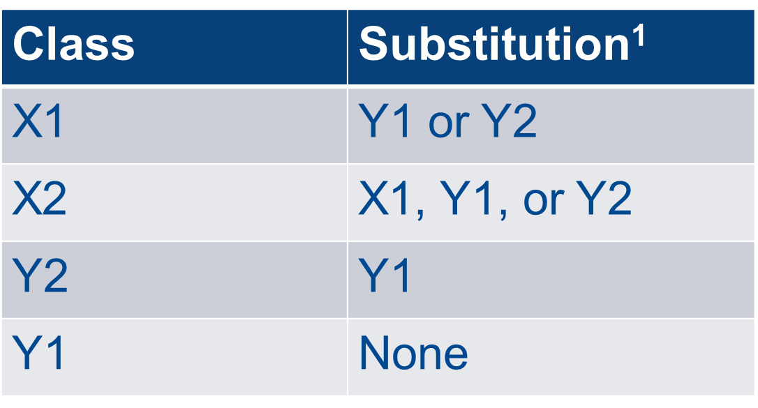
1Substitutions are of the same or higher voltage rating.
Can safety-certified capacitors be used in DC voltages?
IEC 60384-14 defines that all safety-rated capacitors have a DC safety rating equal to the AC rating.
i.e., a 250VAC safety-certified capacitor would have a 250VDC rating.
Can safety-certified capacitors be used above their rated voltage?
The operating voltage for safety capacitors must always be their rated voltage or less. Although the operating voltage is fundamentally what the part should operate under in normal conditions, these capacitors must be designed to mitigate impulses from being passed down the circuit. Considering this, one should also ensure that the class is properly chosen to account for the correct impulse voltage. These capacitors are not meant to be used in conditions that imply higher operating or impulse voltages than what is specified and approved via the IEC 60384-14 specification. Failure to adhere to these directions could imply a risk of fire or shock, depending on the orientation/application of the capacitor, Class-X or Class-Y.
Is the moisture sensitivity level different for Safety Certified disc products compared to SMD?
Yes, KEMET Electronics denotes our safety-certified disc products to have an MSL rating Level 2. Please see the table.
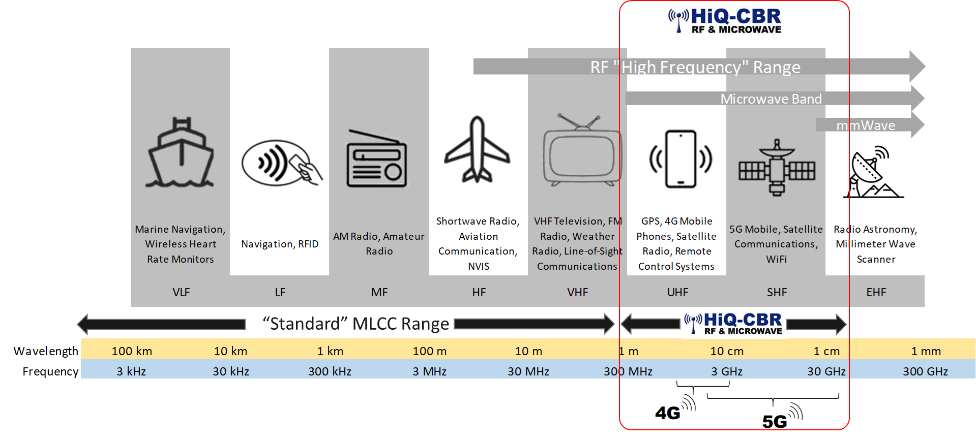
HiQ High Frequency RF Capacitors (CBR Series)
What does RF Stand For?
RF stands for Radio Frequency, which has a frequency range of 30kHz – 300GHz. However, when referring to RF capacitors, the frequency range is usually 300MHz – 50GHz. Below 300MHz, standard MLCCs are suitable.
What is an RF Capacitor?
An RF capacitor is a capacitor whose “characteristics” are optimal at RF frequencies.
Therefore, for RF capacitors, materials are chosen, and designs are optimized so that the capacitor's characteristics are optimal at higher frequencies.
What are typical applications for RF capacitors?
RF MLCCs are used for bypass, coupling, filtering, impedance matching, and DC blocking.
Typical applications include:
RF power amplifiers (PA)
Cellular base stations (4G, 5G)
Wireless LAN
Telecommunication Networks
GPS
Bluetooth
Radar
Automotive V2X, Safety Systems, Power Train, Communication Systems
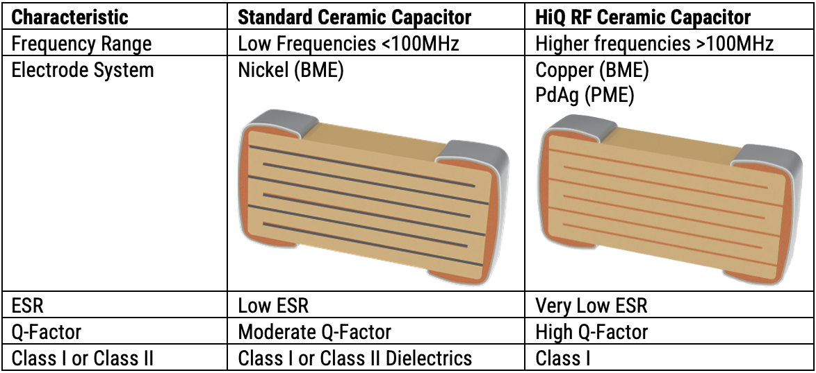
What is the difference between standard Ceramic Capacitors and HiQ RF capacitors?
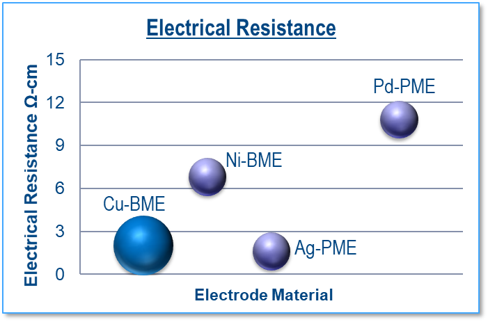
Roughly 99% of all ceramic capacitors shipped yearly are Base Metal Electrode systems with nickel inner electrodes. Since RF capacitors require very low loss at high frequencies, the internal electrodes are either Palladium Silver for Precious Metal Electrode (PME) systems or Copper for Base Metal Electrode (BME) systems.
Since nickel is ferrous, its resistance increases dramatically at higher frequencies than copper. The bottom left plot below shows the resistance of a 1.5mm diameter wire made from copper and nickel versus frequency. The plot shows that the nickel wire's resistance starts increasing above 10MHz, while the copper wire's resistance increase is negligible in the GHz frequency range. Therefore, nickel electrodes are not preferred for RF capacitors.
In some RF capacitors, PdAg may be used, which does provide good ESR at higher frequencies. However, with the increasing costs of precious metals, copper-based RF capacitors provide an outstanding balance of excellent RF performance at a competitive cost.
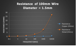
The KEMET CBR series utilizes copper electrodes to maintain very low losses at high frequencies.
What makes KEMET CBR Automotive Grade RF capacitors automotive grade?
KEMET CBR Automotive Grade RF capacitors utilize the same dielectric and electrode materials as the standard CBR series. However, the automotive grade CBR series is qualified, manufactured, and tested per the stringent AEC-Q200 automotive standard.
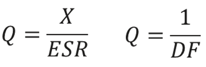
What is Q or Quality Factor, and how does it relate to Dissipation Factor?
Q or quality factor represents the efficiency of a capacitor. It is the ratio of energy stored in a capacitor to the energy dissipated as thermal losses due to the equivalent series resistance (ESR) and I2R losses. Higher ESR can cause excessive heating in the capacitor at higher frequencies beyond its max allowable power dissipation. Since Q is inversely proportional to ESR, lower ESR at high frequencies will have higher Q at high frequencies. Therefore, higher Q capacitors are preferred by RF designers for high-frequency applications.
Q is also related to Dissipation Factor, as seen in the equation below. For lower-frequency applications, DF is traditionally used instead of Q.
What are S-Parameters, and how do I obtain them?
S-Parameters or scattering parameters are used to describe how RF energy travels through a network (filter, amplifier, capacitor, etc.). As an analogy, S-Parameters can be compared to light traveling through a pair of glasses. Some light reflects off the lens toward the source, some travel through the lens to the eye, and some light is absorbed by the lens. Similarly, RF energy can be thought of as a traveling wave. Some waves will bounce back toward the source, some will travel through the network, and others will be absorbed. S-Parameters are a convenient way of quantifying those characteristics of the network.
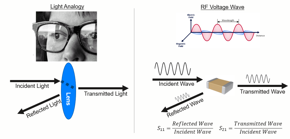
S-Parameters are important in RF design because they are relatively easy to measure and work well at high frequencies versus other parameters that are derived from direct voltage and current measurements. They can be used to characterize not only capacitors but also inductors, transistors, PCB traces, amplifiers, and even complex systems.
How to obtain S-Parameters for the KEMET CBR series?
S-Parameters are provided as a text-based ASCII file and downloaded from the KEMET website.
Do I need to be concerned with PCB and pad dimensions when using RF capacitors?
When MLCCs are mounted to PCBs, the discrete component becomes part of an electrical system consisting of other components and materials. The capacitor does not operate independently from the other components and materials, but they may influence the overall properties. When we mount any ceramic capacitor to a PCB, parasitic effects will be due to the PCB and pad dimensions that need to be considered in the electrical performance. For example, the pad dimensions and ceramic electrodes will have some parasitic capacitance to the ground plane of the PCB, and the pad dimensions will have some parasitic capacitance between them. The inductance (or ESL) is also a function of the PCB properties. For example, thinner PCB substrates will cause the inductance to be lower since the ground plane of the PCB acts like a shield of a conductor.
Why is this important?
Since the parasitic capacitances and inductance of MLCCs are relatively low at low frequencies, it is not of much concern. Even though the PCB and pad dimensions have some influence on the electrical characteristics, at lower frequencies, they are usually negligible. However, at higher frequencies, these parasitics start influencing the capacitor properties, becoming a significant consideration in the overall design. Here, we can see an example of S11 for a 5.6pF 0805 RF capacitor up to 10GHz mounted on three different PCBs. Notice after about 800MHz, S11 for all three PCBs starts deviating from one another considerably.
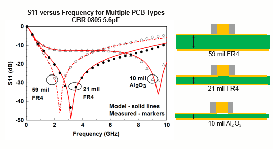
This example shows just how important taking into consideration PCB conditions can be.
There is one limitation with S-Parameter data. S-Parameters are data from a single capacitor measured under a single PCB and pad dimensions. Therefore the actual performance of the RF capacitor can be different from the customer's actual use conditions, so designers need to consider the effects of PCB and pad dimensions.
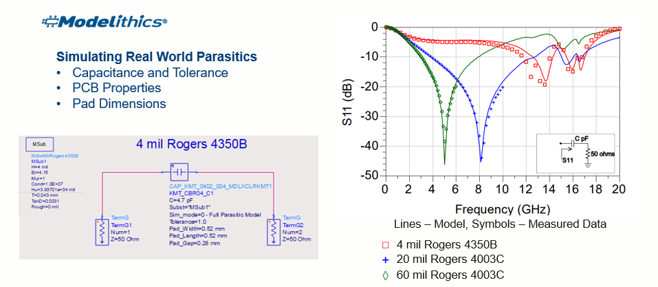
What are Modelithics Models, and how do I obtain them?
To help customers design in the KEMET CBR RF capacitor series, KEMET has partnered with Modelithics to provide customers with scalable substrate models that can be downloaded and simulated in popular EDA design tools. These measurement-based models allow designers to input capacitance value, tolerance, pad dimensions, and PCB information. The result is an entire substrate scalable model that accurately predicts the behavior of the actual PCB performance to achieve first-pass-design success.
Please visit to inquire about obtaining KEMET Modelithics Models for the CBR series. (LINK)
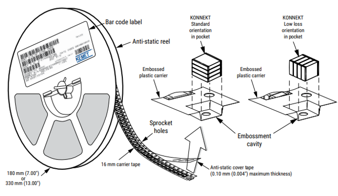
KONNEKT Technology
What is KONNEKT™ Technology?
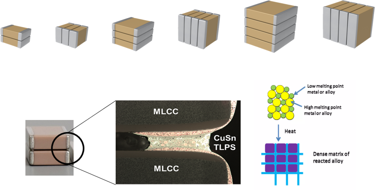
KONNEKTTM is a patented high-density packaging technology that allows MLCCs to be bonded together without the use of metal frames. KONNEKT technology utilizes innovative transient liquid phase sintering (TLPS) material which has low temperature reaction of low melting point metal or alloy with a high melting point metal or alloy to form a reacted metal matrix. The result is a highly conductive bonding material that can be used to connect multiple MLCCs together to form a single surface mountable component.
Is KONNEKT™ Technology Pb-Free and RoHS Compliant?
Yes, KONNEKT Technology is 100% Pb-Free, RoHS and Reach Compliant with no exceptions.

Why does KONNEKT™ use TLPS and not metal frames?
Metal frames add ESR, ESL, and thermal resistance to capacitors, reducing their power handling capability. Since MLCCs are often used in high power applications such as wireless chargers and resonant converters, reducing these losses is critical to minimize self-heating. KONNEKT technology allows for the lowest ESR, ESL and thermal resistance possible in the form factor.
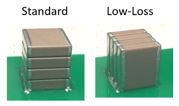
What is the difference between Standard and Low-Loss orientation?
The terms “Standard” and “Low-Loss” refer to the orientation of the KONNEKT stack when mounted to a PCB. In standard orientation, the MLCCs are parallel to the PCB plane. In Low-Loss orientation, the MLCCs are perpendicular to the PCB plane.
Low-Loss orientation enables higher power handling capability by lowering the ESR (Effective Series Resistance), ESL (Effective Series Inductance), and Thermal Resistance (Rth). This makes the Low-Loss orientation of KONNEKT the ideal choice for high power density applications such as wireless chargers and resonant converters.
EIA 3640 KONNEKT in Standard and Low-Loss Orientation
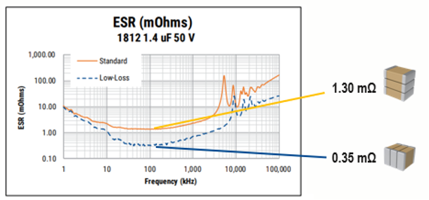
Typical ESR for U2J with KONNEKT 1812 1.4uF 50V
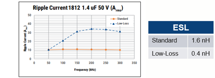
Typical Ripple Current and ESR for U2J with KONNEKT 1812 1.4uF 50V
Why are some KONNEKT capacitors available in standard orientation but not Low-Loss?
KEMET offers KONNEKT technology in Low-Loss orientation to reduce ESR, ESL, and thermal resistance. However, in some cases, Low-Loss orientation is not practical given the aspect ratio of the MLCCs and therefore is not offered. For example, CKC33C444KCGLCAUTO (KC-LINK with KONNEKT, 2-Chip, EIA 3640, 440nF, 500V, K Tolerance) is only available in standard orientation as seen below.
KC-LINK with KONNEKT, 2-Chip, EIA 3640 in Standard Orientation
See KEMET KONNEKT datasheets for details on product offering.
Is there a difference between the materials or construction of standard orientation KONNEKT capacitors versus Low-Loss orientation?
No, the material and construction between standard orientation and low loss orientation is identical. The terms “Standard” and “Low-Loss” refer to the orientation of the KONNEKT stack when mounted to a PCB. In standard orientation, the MLCCs are parallel to the PCB plane. In Low-Loss orientation, the MLCCs are perpendicular to the PCB plane. Before shipping the capacitors from the KEMET manufacturing facility, the KONNEKT capacitors are placed in either standard or low loss orientation in the Tape and Reel pocket. This allows the capacitors to be Pick-N-Placed in the correct orientation.
What are the recommended soldering techniques for KONNEKT capacitors?
See link below for KONNEKT Mounting Recommendations document for pad geometry, solder reflow, wave soldering, and hand soldering guidelines.
How are KONNEKT capacitors tested for vibration?
KEMET KONNEKT capacitors are tested using the following test conditions:
MIL-STD-202 Method 204
5 g for 20 minutes, 12 cycles each of 3 orientations. Note: Use 8” x 5” PCB 0.031” thick 7 secure points on one long side and 2 secure points at corners of opposite sides. Parts mounted within 2” from any secure point. Test from 10 – 2,000 Hz.