KEMET’s original digital flame sensors employ a surface mount footprint with 8 pins, providing additional signals which allow greater flexibility for the design engineer.
This application note covers the required hardware and operational requirements of the KEMET QFCE sensor when only 4 pins are used (compared to the QFS and QFSM series).
Operational differences arise from the reduction of pins available on the TO-39 package. Therefore, the method of operation is required to change to facilitate correct operation. This document covers some options for the additional surrounding circuitry. It should be used in conjunction with the corresponding document Application Notes – Digital TO39 QFCE Series TO Software for the software differences and the document SMD Sensor Reference Manual.
The digital range of thin-film pyroelectric IR sensors combines high performance with a high level of configurable electronic integration in the smallest SMD package or a TO39 package.
KEMET’s QFCE pyroelectric flame sensors combine high sensitivity with fast response times and high dynamic range to ensure rapid and accurate detection of small and large flames, nearby or over larger distances.
These high-sensitivity flame detectors integrate digital front-end circuitry to provide all associated analog electronics required for sensing flame events. These events can then be interpolated by direct connection to a microcontroller. All of this occurs in an industry-standard TO39 package.
The thin-film PZT substrate allows industry-leading response times providing high responsivity over the entire frequency of flame flicker from 3 to 30 Hz. The industry-standard I2C communication interface provides plug-and-play connectivity to microcontrollers. It also allows easy tuning and calibration via programmable gain and filtering, offering maximum flexibility at the system design level.
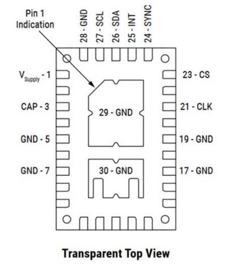
Figure 1 – Digital SMD Sensor
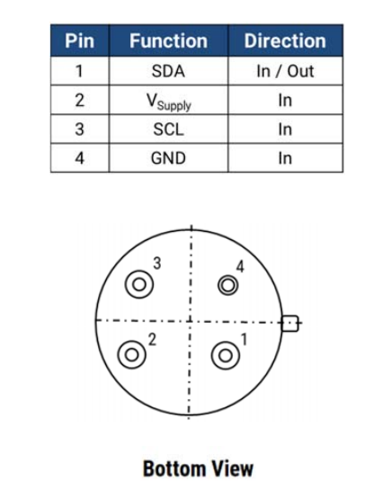
Figure 2 – Digital TO Sensor
The above figures show the connections available for KEMET’s SMD or TO digital sensors. The digital TO is functionally equivalent to the SMD version used with only 4 pin connections. The TO package only allows for V+, GND, and the I2C lines. This means that the following pins that can be used in the SMD version of the sensor are not accessible.
1. INT |
2. SYNC |
3. CLK |
4. CS |
The following sections describe the use of these pins and the impact of the restricted number of pins on the reduction in functionality.
The INT pin on the SMD sensor indicates to the attached MCU that there is data available in the FIFO and ready to be read out using the appropriate I2C command. The lack of access to the INT pin means that the FIFO must be checked using the FIFO status command.
The FIFO status packet, as described in Section 13.3.3 FIFO Status Packet of the SMD Sensor Reference Manual, contains the interrupt pins status in bit 0 of the returned byte and can be used to poll the FIFO status. Also, this implies that any Sleep/Wake-up function needs to be done by polling.
Figure 3 shows the logic analyzer results from during normal operation of an SMD sensor that has access to all the pins.

Figure 3 – Interrupt Pin Operation Mode
The interrupt pins all go low simultaneously due to the daisy-chaining of the devices with the sync signal from the master making all sensors take a sample. As data is read out from each device and then the FIFO cleared, the INT lines go low one at a time. The I2C commands to read the data out begin once the MCU has detected the INT line states.
Figure 4 shows the FIFO status being checked to determine data availability.

Figure 4 – FIFO Status Polling Operation
The above figure shows three FIFO status checks that return a FIFO status corresponding to no data and then a final FIFO status check that indicates there is data available, followed by reading the data out and clearing each FIFO in turn.
These pins on the SMD sensor synchronize sampling between multiple sensors. Under 4 pin operation, each sensor uses its internal CLK and SYNC signals, so every digital TO sensor must be set up as a master by configuring the AFE register as described in the SMD Sensor Reference Manual, in Section 13.3.5 Analog Front End Packet.
This configuration has the effect of removing the ability to daisy chain the sensors. They are independently clocked devices.
The chip select pin is also not available in 4 pin-connected sensors. The CS is wired internally directly to the positive voltage input on the digital TO sensor. Thus, the CS signal goes high when the voltage supply is turned on.
If multiple sensors are being powered from the same supply, there needs to be a way to re-address the devices separated by powering them on in sequence. This sequence is discussed in Section 3.2 of this document.
On the KEMET digital TO flame sensing evaluation kit USEQFCK9000000, the digital output from the MCU controls a separate power switch for each of the sensors connected to the MCU. If any individual flame sensor requires a reset, these power switches facilitate control over individual sensors.
If the MCU is reset, then all flame sensors should be reset at the same time. The sensor power switch should ensure that the VDD pin is pulled to the ground rather than left floating. A floating supply does not allow correct reset timings within the sensor and, therefore, can have adverse effects if not controlled correctly.
The power switch schematic is shown in Figure 7. There are connections to this in both Figures 6 and 8.
In addition to controlling the power for each sensor, the I2C CLOCK pin must also be controlled. This requirement occurs due to the lack of Chip Select (CS) signal on the digital TO-39 package.
If multiple sensors are used on the same communication bus, then each device will be required to be reprogrammed to have a unique I2C address. This is performed by controlling each I2C clock line to individual sensors. The control over the clock line also prevents the devices from being powered from the I2C bus when the power to the sensors is reset.
On our QFS and QFSM series of SMD devices, the sensors are initialized by setting the CS of one device at a time and re-addressing each device until all sensors have distinct addresses on the I2C bus.
The operation of the digital TO-39 devices is different as there is a single power switch for all sensors. The solution is to use a chip that can allow or deny access to the I2C clock signal to each sensor. Although the data is going to all sensors, the I2C hardware is not being clocked and the incoming data is not being read.
With this additional piece of hardware, the same code for the digital demo board can be used since the same signals used to activate chip select are used to control sensors receiving the I2C clock.
If multiple sensors are used on the same I2C bus, each device requires a unique I2C address. Proper operation can be achieved by performing the following sequence.
Ensure the sensors have been correctly reset, then using control over the I2C clock lines, disable all devices for which you are not trying to reprogram the associated I2C address.
Reprogram the I2C address according to the SMD Sensor Reference Manual and your required address. Once completed, leave that device powered on and re-enable the I2C clock line to the next device in the chain you intend to program. Follow this procedure for each device on the I2C bus, ensuring each device in the chain has a unique address.
KEMET sensors do not contain Flash memory, so every time the power to the sensors is disrupted, you should ensure that you reset and reprogram each individual I2C address. Failure to reset or reprogram the devices will result in random failures when reading or writing data to each sensor.
With the digital SMD sensors, there are various methods for the MCU to determine whether there is data in the FIFO.
1. Use INT pin of the sensor and Interrupt within the MCU.
2. Use INT pin of the sensor and Poll it with the MCU.
3. Use the I2C FIFO_Status command and check the bit corresponding to the INT status. Performing this is effectively polling the FIFO_Status.
Since the first two require the INT pin of the sensor, they cannot be used in 4 pin operation, the only method of checking whether there is data in the FIFO is to use the I2C FIFO_Status command.
It is worth reminding here that when polling the FIFO_Status, the I2C bus is being used. Therefore, the frequency of checking the FIFO_Status should be kept to a minimum to improve power usage.
For example, this has been accomplished in the digital TO evaluation kit through an interrupt that uses the current sampling rate and power mode to determine its frequency of checks.
The lack of synchronized sensor sampling produces the following result in the FIFO polling data read-out mode. The narrowest I2C packets correspond to none of the sensors having data in the FIFO, and the widest packets correspond to all sensors having data in the FIFO. The other I2C packets correspond to FIFO status checks that have returned only a subset of sensors with data available.

Figure 5 – FIFO Polling – Effect of Unsynchronized Sampling
Since the sensors are independently clocked, the point at which data is available for each sensor is different. Care must be taken when designing the firmware to read the sensors to avoid losing data.
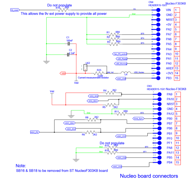
Figure 6 – MCU Connections
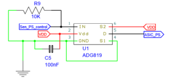
Figure 7 – Power Supply Switch
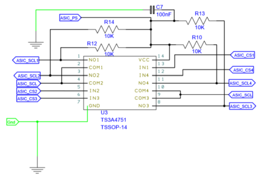
Figure 8 – Sensors Clock Switches
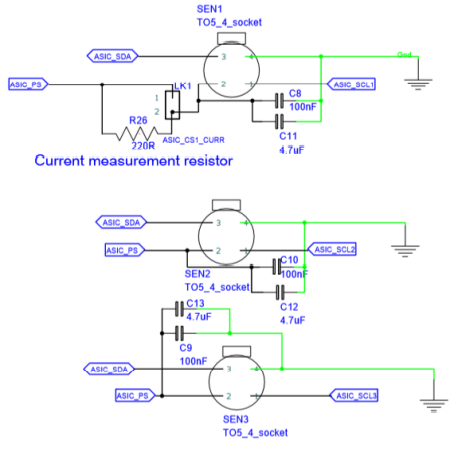
Figure 9 – Digital Sensor Sockets
Developers should note that the I2C pull-ups and the I2C clock switch receive their 3.3 V from the output of the power supply switch (controlled via the MCU).
The result is when the digital sensor does not have a 3.3 V applied to its VSupply pin. Then the other digital IO pins can feed onto the 3.3 V rail of the sensor’s ASIC through internal protection diodes. However, if there is no 3.3 V supply, then any voltage over 0.6 - 0.7 V on the other pins is fed onto the 3.3 V rail, and hence the device could be powered through the I2C lines. To avoid this, they are kept low until the 3.3 V signal is supplied.
The above descriptions are for the current version of the KEMET demo board. This example was chosen to reduce the component cost. However, it does mean that the lowest current consumption for sleep mode is not achievable.
In low power applications, the individual control over power and clocks to each sensor will drastically reduce the power consumption of the final application.
The kit should only be actively analyzing the data if the flame sensor is above some threshold value, considering the digital TO flame sensing evaluation kit’s expected usage as an example of the differences in power consumption performance for a different circuit choice. It is implied that the sensors can be asleep and use the wake-up parameters described in Section 13.3.7 of the SMD Sensor Reference Manual. If you are unfamiliar with the WUP packet, it is recommended to use the Flame Sensing Evaluation Tool (Digital) software as it contains a useful visualization aid to setting up and testing the parameters. This Evaluation Tool software is available to download here.
As mentioned above, the Flame Sensing Evaluation Kit should ideally be asleep most of the time unless an event considered to be a fire is detected on the sensor output. In this event, if the signal level is just noise, the devices should remain asleep. The WUP packet determines the necessary level of signal for a wake-up condition. If all three devices are sleeping on the digital TO Flame Sensing Evaluation Kit, then the minimum current consumption of the sensor system sits at around 18.2 µA. However, since the interest is only in the flame sensors signal to determine a wake-up event, the other two devices could be powered down. This scenario would put the sleep state current consumption at 7.3 µA.
The downside to the above reduction to the lowest current consumption is the additional hardware cost. Section 3.4.1 of this document shows that the I2C cannot be connected to a powered-down device. Otherwise, the 3.3 V feeds onto the Vcc rail of the sensor through protection diodes. Therefore, if each device can have power independently, it also needs to have the I2C lines only connected when it has power. This operation will avoid problems with registers not initializing correctly in the ASIC. This operation implies that there should be a single power and two I2C signal switches per sensor.

Table 1 – Component Cost and Corresponding Current Consumption
Here are two examples of possible solutions:
Analog Devices: ADG819BRTZ-500RL7
Texas Instruments: TS3A4751PWR