There is a long-established market for high temperature multi-layer ceramic capacitors (MLCC) that operate at 150°C and higher in down-hole oil & gas exploration, military and aerospace applications. To maximize the capacitance density and achieve a high degree of mechanical robustness, stacks and leaded form factors have been used with High Melting Point (HMP) Pb-containing solders as the preferred interconnects. However, Pb-containing solders are limited to temperatures below 300°C and are banned from many commercial and automotive applications with further legislation limiting their use planned in the future. Common Pb-free solders such as SAC 305 or SnSb alloys are in widespread use but their performance at prolonged exposures at 200°C is limited. Exposures to high reflow temperatures during assembly, especially successive reflow operations, can also compromise interconnect integrity. Higher temperature gold-containing solders are widely available but these are cost prohibitive and so are not viable for emerging high temperature electronics including higher volume, price sensitive Automotive and Power markets. The development of more energy efficient power converters and inverters based on Wide Band Gap (WBG) semiconductors is driving the adoption of higher temperature electronics in these markets since these operate at higher junction temperatures than traditional silicon. This has led to the development of non-solder interconnects based on sintered silver, nano-metal sintering and transient liquid phase sintering (TLPS) technologies capable of higher temperature performance than common solder based interconnects. The availability of discrete components, such as capacitors, that can operate under these conditions is a key barrier to the development and adoption of high temperature electronics. In this paper the key property differences between solders and TLPS interconnect technologies are compared in detail for MLCC interconnects. The development of a new range of nickel Base Metal Electrode C0G MLCC stacks rated for 200°C is described and performance compared to traditional Precious Metal Electrode (PME) stacks. Thermal cycling performance to 200°C of BME X7R stacks made with 10Sn/88Pb/2Ag solders are compared to similar stacks made with TLPS interconnects of Cu-Sn and In-Ag. The development of leadless stacks, a new bulk capacitance form factor enabled by TLPS technology, is described and their properties compared to traditional stacks.
Key words: High-Temperature Interconnects, Multi-Layer Ceramic Capacitors, Transient Liquid Phase Sintering.
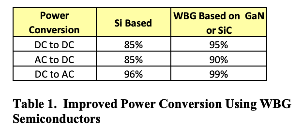
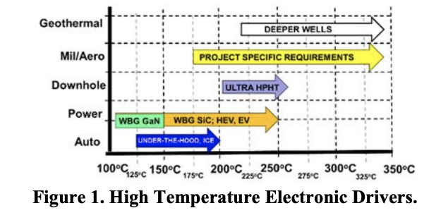
The oldest and largest user of high temperature electronics (≥ 150°C) is in downhole oil and gas exploration. In the last few years the low cost of oil, around $50/barrel or less, has reduced the level of activity in the development of the associated high temperature electronics in these applications. More recently there is increased interest in real time sensing and automation require more use of electronics. Furthermore, the Shell Oil Company have announced its intent to develop budget deep-water drilling [1]. This will likely involve moving to ultra High Pressure High Temperature (uHPHT) wells defined as 138MPa and 205o C [2] requiring a further upgrade in the electronics required. The Geothermal, Military and Aerospace markets can require even higher temperature electronics but these are usually value added custom applications that can support higher prices. The increasing amount of electronics content in Autos made with internal combustion engines (ICE) has forced more electronics incorporation under-thehood. These temperature requirements often exceed 150°C which has led many Tier 1 suppliers to require components to be upgraded for use at these higher temperatures above the recommended ratings. There is also increased development activity associated with hybrid and electric vehicles (HEV/EV). The availability of cheaper of wide band gap (WBG) semiconductors based on GaN and SiC that can offer more efficient energy conversion [3] is further disrupting this market space as well as in mainstream power electronics. The improved efficiencies compared to silicon are shown in Table 1.
Higher switching frequencies associated with WBG help miniaturize the power supplies [4]. Silicon carbide can operate at very high junction temperatures > 200°C and voltages ≥ 650VDC but availability of suitable capacitors is limiting progress toward commercialization. In many of these industrial and automotive applications a key concern is how to manage the heat generated [5]. Traditional cooling techniques may not be effective for standard passive components, such as metallized polypropylene film capacitors, that are limited to a maximum temperature of around 105o C. One approach is to upgrade the cooling to enable the use of more standard components but there is also great interest in moving to higher temperature passive components capable of operation at 150°C and higher. These high temperature electronics drivers are depicted in Figure 1.
An analysis of different capacitor types rated 200°C in different manufacturers catalogs was previously performed [6] and is reproduced in Table 2 for different voltage ratings.
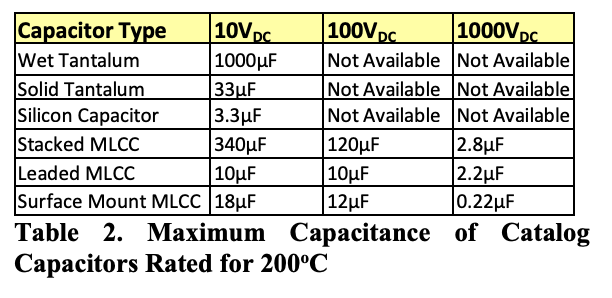
The list of capacitor types only includes those supported in catalogs so excludes some specialty types such as high temperature film capacitors. In this survey the rated voltage at 200°C has been used together with the nameplate capacitance. By example extensions of solid tantalum capacitors can now reach 220µF in 10VDC ratings at 85°C but these require significant de-rating to 3.3VDC at 200°C. High voltage ratings of ≥ 100VDC are only available in MLCC catalog parts. Furthermore, to achieve a high capacitance in a single component it is necessary to use a stack or leaded MLCC. However, in these high voltage ratings the nameplate capacitance can be misleading since they are based on Class II, X-type MLCC (EIA 198-D) that lose capacitance under applied voltage and temperature rather than more stable Class I dielectrics. By way of an example we compared the performance of the same stacks of 0.27µF 500VDC rated 3 x MLCC Case Code 5 Class II X-type stack from a competitor with a similar size 0.15µF 500VDC stack made with our Class I Ni BME C0G technology. The capacitance at 500VDC is compared for these stacks over the temperature range -55 to 200°C in Figure 2.
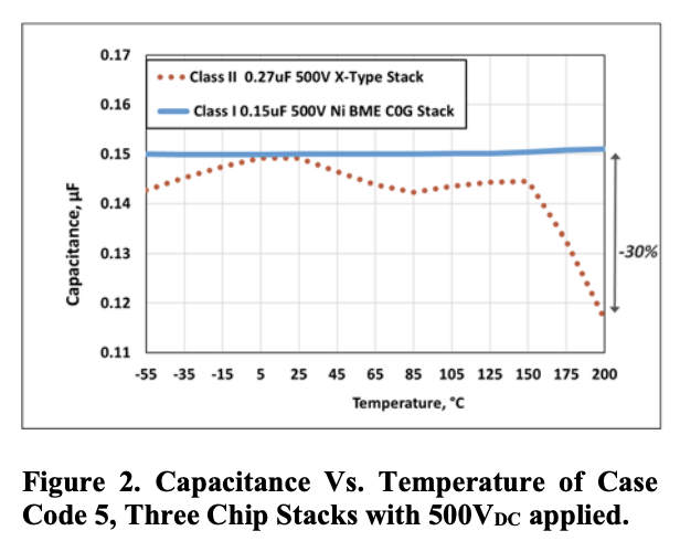
Although the nameplate capacitance of the X-type stack is 0.27µF at 1VAC, 1kHz when 500VDC is applied this drops to the same value as 0.15µF Ni BME C0G stack. As temperature is increased to 200°C the X-type stack capacitance drops further to 30% less than the C0G capacitance that is unaffected by temperature and voltage.
These high voltage stacks are often used in power applications where they can be exposed to significant AC voltages. It is well known that applying AC voltage to MLCC can cause them to heatup. The power dissipated during this ripple current self-heating is directly proportional to the ESR and current applied:
The ESR of these stacks was measured at select frequencies from 10kHz to 500kHz and the power dissipation calculated for 3ARMS as shown in Table 3.
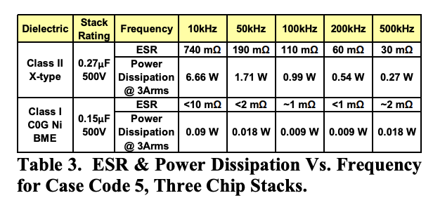
The ESR of the C0G stack is far lower than the X-type resulting in far less heat dissipation over this broad range of frequency. To confirm this evaluation the self-heating at 100kHz was measured on the top MLCC of each stack for various applied currents as shown in Figure 3.
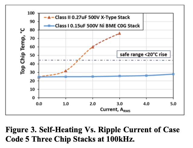
The X-type stack rapidly heats-up exceeding 20°C, usually considered safe, around 1.5ARMS whereas the C0G stack barely heats up at all.
In high temperature operation, the thermal and mechanical robustness of these stacks is a concern with respect to meeting user mission profiles. High melting point (HMP) Pb-containing solders are the most common lead interconnect material for 200°C ratings, as in these 2 different stacks, and the performance of solder interconnects is reviewed below.
The temperature capability of some selected solders is summarized in Table 4.
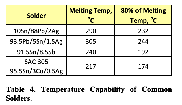
The Pb-free solders have melting points close to 200°C (Table 2.) and their shear strength rapidly declines above this temperature, Figure 4, as previously reported [7].
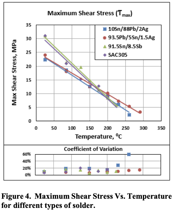
These comparisons were performed with case size 4060 (0.40” x 0.60”) tin plated MLCC with two leads approximately 0.23” wide and 0.01” nominal thickness soldered to each side of the MLCC. The Pbfree solders lower shear strength at higher temperatures combined with limited safety margin between melting points and 200°C makes their use problematic for continuous applications at this temperature. Therefore, in applications at 200°C and higher stacks and leaded capacitors use HMP Pbsolder interconnects. Another key performance parameter for the robustness of these interconnects is their ability to survive temperature cycling. To prevent early failures due to solder fatigue the strain on the interconnect should be minimized. Accelerated cycling data -40°C to 240°C with 48°C/min transition and 15 minute hold at these temperatures was used to investigate 10Sn/88Pb/2Ag solder interconnects for various lead designs to minimize the stress levels. The shear stress at 200°C is compared for a low and high stress combinations exposed to 300 and 600 cycles in Figure 5.
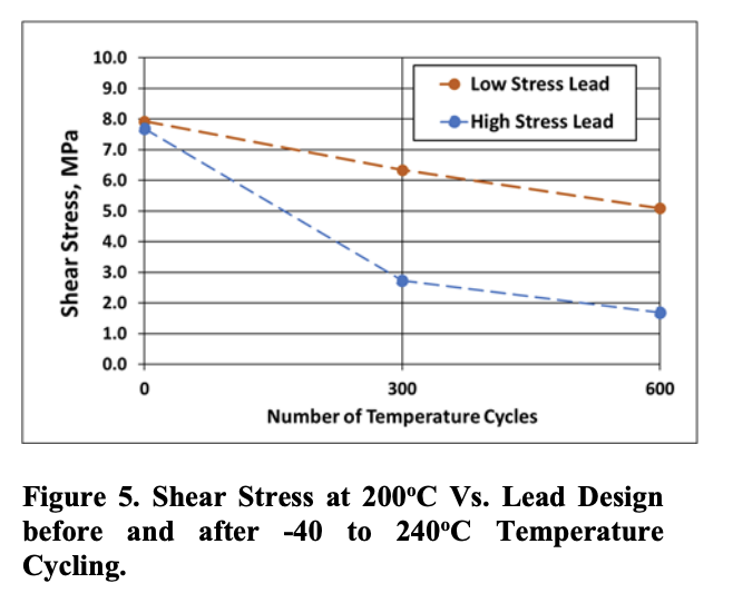
In both the cases shown (Figure 5) complete failure of the interconnect due to solder fatigue did not occur. However, examination of the detached leads after 600 cycles shear testing showed peripheral detachment due to solder fatigue.
The low stress lead lost 36% of its shear strength after 600 cycles compared to 79% loss for the high stress case. The low stress lead design elements were applied to 200°C rated Military Case Code (MCC) Ni BME C0G stacks. These were subsequently qualified through 400 cycles of -40 to 240°C with no failures allowed and life tested at rated voltage for 1000 hours at 200°C as documented in Table 5.
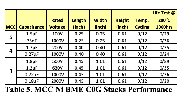
These large case stacks have reliable performance at 200°C with no failures in this range recorded in 314,000 test hours (35.8 years) at this temperature and their respective rated voltages.
HMP Pb-containing solders (>85% Pb) used in these interconnects are still exempted in EU RoHS 2 regulations for Industrial Applications and Mil/Aero. However, these exemptions are under threat of withdrawal, in some cases as early as 2021. Furthermore, Pb-solders are banned from many Automotive and Commercial applications so there is a desire to develop viable alternatives to enable the use of high-temperature capacitors in mainstream electronics.
The attributes of potential alternative interconnect materials are assessed with respect to some desired targets for MLCC products as shown in Table 6.
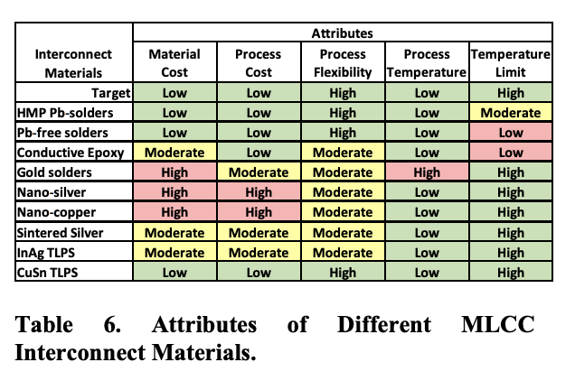
Gold solders along with nano-silver or nanocopper are considered too expensive for MLCC interconnects. Conductive epoxy, already, used in some lower temperature rated leaded MLCC products, has limited temperature capability. Sintered silver and transient liquid phase sintering materials have been successfully applied to semiconductor packages and appear relatively cost effective. InAg TLPS bonds have been manufactured in a fluxless bonding process [8]. In this case the TLPS is formed through interdiffusion of thin layers deposited on flat surfaces to form a void free metallurgical bond suitable for die attach. Initially we attempted to form lead-to-MLCC interconnects by inter-diffusion of plated layers but this could not be applied successfully to our relatively non-planar MLCC terminations. To bond these uneven surfaces combined and achieve high shear capability for mechanical robustness we developed TLPS interconnects based on pastes [9]. Subsequent development of the paste technology was done in collaboration with Ormet Circuits, Inc., a subsidiary of Merck KGaA, Darmstadt, Germany. These TLPS materials have been exploited in a variety of electronic applications including wafer packaging [10]. Sintered silver is used by competitors in 150°C rated leaded MLCC. In this case the area of the sintered silver interconnect is 0.104” x 0.209” and further examination showed the presence of additional polymeric bonding material. To understand the potential for sintered silver interconnects the shear strength Vs. % shear strain is compared to 10Sn/88Pb/2Ag solder and CuSn TLPS lead interconnects both with area of 0.08” x 0.23”in Figure 6.
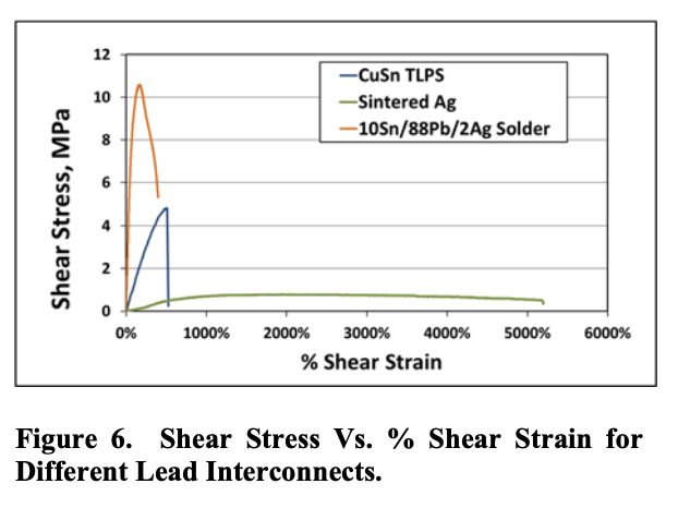
The Sintered Silver has very low shear stress with extensive elongation and so resembles a weak adhesive bond. There were no measurements of the integrity of the MLCC connection during these shear tests but clearly the CuSn TLPS more closely resembles the Pb-solder. Our work therefore focused at an early stage on developing Transient Liquid Phase Sintering (TLPS) materials and processes.
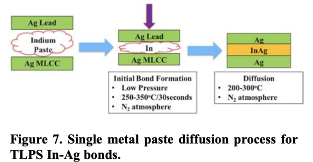
Two different TLPS interconnects were developed based on CuSn and InAg. Both are applied as pastes and then heated at 250-350°C to form metallurgical bonds between the MLCC and the lead. The InAg TLPS bond is formed by diffusing indium from a paste into silver on the lead and MLCC termination, a single metal paste diffusion process [6] as shown in Figure 7.
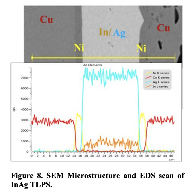
The Indium is diffused to give a uniform alloy containing 80% Ag (Figure 8.)
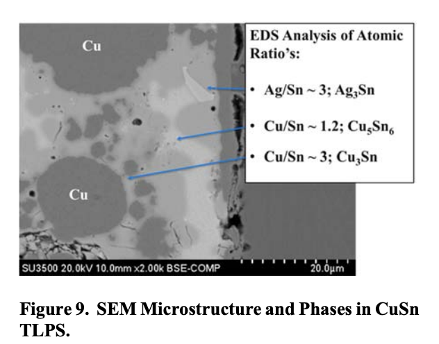
The appearance of the metallurgical bonds in CuSn TLPS is very different. The CuSn TLPS paste forms a mixed metal composite during the initial bonding process with no further diffusion stage required. This can form bonds between Sn, Cu Ag and Au surfaces. There are excess Cu spheres present in a matrix of CuSn phases (Figure 9.).
The work done to deform a solid when a force is applied is proportional to the magnitude of the applied force and the amount of deformation, and is stored in the solid as potential energy. When the force is a shear force, the energy stored is referred to as shear energy. Materials that have higher ductility in shear can store larger amounts of shear energy. The shear energy at different temperatures was recently compared [11] for 2220 case size leaded MLCC made with these TLPS materials and to 10Sn/88Pb/2Ag and 91.5Sn/8.5Sb solders interconnects (Figure 10.).
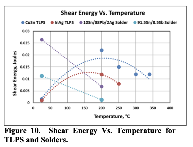
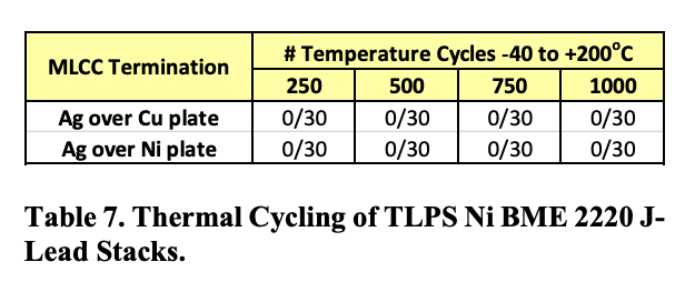
The TLPS materials retain high shear energy above 200°C extending to higher temperatures than these solders. Single MLCC of case size 2220 Ni BME C0G with plated silver capacitor terminations over Cu and Ni underplate respectively were bonded to silver plated Phosphor Bronze J-leads made with InAg interconnects [11]. Temperature cycling from -40 to 200°C with a 48°C/min ramp rate between temperatures and a 15-minute hold at each temperature was performed on 30 piece samples of each type (Table 7.).
Thermal cycle performance of TLPS materials was also compared to 10Sn/88Pb/2Ag solder interconnects for multiple capacitor stacks consisting of twelve (12) 1812 case size MLCC. These 40µF stacks were made using 25V 175°C rated 3.3µF Ni BME X7R MLCC. MLCC surface finishes of tin, electroplated copper, and electroplated silver evaluated with CuSn TLPS interconnect as well as electroplated silver finish with the InAg TLPS. A high-Pb hot solder dip MLCC finish was used in combination with the 10Sn/88Pb/2Ag solder interconnect. In addition, two types of lead frame base metal were used that have different temperature coefficients of expansion. The CTE of Phosphor Bronze is 17.8 while the CTE of Alloy 42 is about 4.5 ppm/°C. An additional combination of immersion gold MLCC finish with CuSn TLPS material was included with the Alloy 42 lead frame-group.
Temperature cycling was performed from -55 to +200°C with 48°C/min transition between temperatures and a 15-minute hold at each temperature, for a total of 200 cycles. The multiMLCC stacks were mounted to polyimide PCB’s to include the additional component of temperature cycling stresses due to expansion and contraction of the PCB. A shift in capacitance or IR of the multiple MLCC stacks was considered a temperature cycling failure. The results of temperature cycling for the multiple MLCC stacks are shown in Table 8.
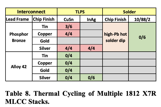
All combinations of CuSn and InAg TLPS made with low CTE Alloy 42 lead frame exhibited no temperature cycling failures after 200 cycles, while all combinations made with Phosphor Bronze lead frame failed temperature cycling. The control group consisting of the high-Pb solder interconnect with Phosphor Bronze lead frame exhibited no failures. This result suggests that low CTE lead frame is required when using TLPS materials to bond multiple MLCCs to lead frames to ensure temperature cycle robustness. This is likely due to the lower ductility of the TLPS materials compared to solder.
These results show that stacks with TLPS interconnects can be made with have robust thermal cycling performance facilitating the replacement of Pb-solders in stacked and leaded MLCC rated at higher temperatures ≥ 150°C.
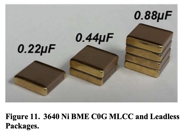
In addition to using TLPS to replace Pbsolders in leaded capacitor interconnects it can be used to bond MLCC terminal-to-terminal to form Leadless Stacks [12]. Since the TLPS based interconnects between the MLCC have high temperature capability the resulting packages can simply be soldered onto boards for increased capacitance on a given pad size area. MLCC of case size 3640 Ni BME C0G have been bonded in this way and tested for use in high power 500VDC 150°C rated capacitors for high current DC-Link applications [13]. Leadless packages of 2 and 4 x 3640 MLCC were manufactured by bonding the thin gold on the MLCC terminations together with CuSn TLPS (Figure 11).
These 3640 MLCC, 2 and 4 chip packages were soldered (SAC 305) onto FR4 test boards and flex tested (Figure 9.).
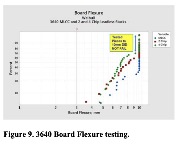
The capacitors can be flexed to > 3mm with no failures and for many test samples no failures were recorded at 10mm. This 3mm requirement represents the minimum for C0G type MLCC qualified to AEC-Q200. Thermal cycling -55 to 150°C was performed on 50 pieces each of the 2 and 4 chip packages with no failures recorded through 1000cycles. The room temperature shear stress was measured on 10 samples of the 2-chip package before and after 1000 cycles as well as after 1000 hour storage at 200°C (Figure 10.).
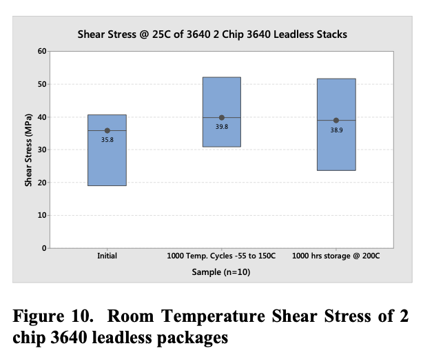
The CuSn TLPS interconnect bonding the 2 chip 3640 MLCC together shows no sign of being degraded by temperature cycling or storage at 200o C. There is no specification for leadless stack shear strength but the minimum board shear requirement of AEC-Q200 Rev D, 2010, Method 006 is 1.8kg. The minimum value recorded for the initial shear strength of 19.1MPa is 27.9kg, over 15 times higher than this requirement. The testing so far indicates the leadless stacks will be a highly reliable form factor to increase the capacitance per pad area in power electronics.
Deeper wells are driving the need for high temperature electronics in the downhole industry. WBG semiconductors for more efficient power conversion based on SiC require higher temperature capable capacitors. Leaded and stacked MLCC have the highest capacitance values at voltages ≥ 100VDC in 200°C catalog ratings. These maximum capacitance values are based on the room temperature values of Class II, X-type dielectrics that loose significant capacitance at higher temperatures and voltages. Higher voltage stacks made with Class I Ni BME C0G can have higher capacitance at 200°C temperatures than similar sized Class II X-type stacks. The C0G stacks also have much lower power dissipation over a broad range of AC frequencies from 10kHz to 500kHz. HMP Pb-solders are currently used to connect the leads in stacks and leaded MLCC. Transient Liquid Phase Sintering (TLPS) materials of CuSn and InAg have been demonstrated as viable alternatives to HMP Pb-solders for high temperature lead interconnects rated at 200°C. These TLPS materials have been used to develop Leadless Stacks, a new form factor, for increasing capacitance within a given pad area.
Scale-up of TLPS technology for Pb-free traditional leaded stacks and leadless MLCC packages is underway. The high temperature capability of these bulk capacitance solutions will allow their application in main stream high temperature electronics with ratings ≥ 150°C.
John Bultitude, John McConnell, Lonnie Jones, Galen Miller,
Jim Magee, Allen Templeton, Abhijit Gurav and Reggie Phillips
KEMET Electronics Corporation
2835 KEMET Way, Simpsonville, SC 29681, USA